background image

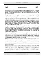
INSTRUCTION DESCRIPTIONS

MOTOROLA 

INSTRUCTION SET DETAILS

A - 103

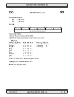
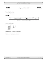
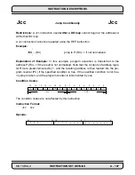
Condition Codes:

The condition codes are not affected by this instruction.

Instruction Format:

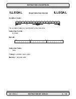
ILLEGAL

Opcode: 

Instruction Fields:

None

Timing: 8 oscillator clock cycles

Memory: 1 program word

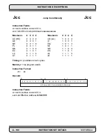
MR

CCR

15

14

13

12

11

10

9

8

7

6

5

4

3

2

1

0

LF

DM

T

**

S1

S0

I1

I0

S

L

E

U

N

Z

V

C

23

16 15

8

7

0

0

0

0

0

0

0

0

0

0

0

0

0

0

0

0

0

0

0

0

0

0

1

0

1

ILLEGAL

Illegal Instruction Interrupt

ILLEGAL

Summary of Contents for DSP56K

Page 1: ...DSP56000 24 BIT DIGITAL SIGNAL PROCESSOR FAMILY MANUAL Motorola Inc Semiconductor Products Sector DSP Division 6501 William Cannon Drive West Austin Texas 78735 8598 ...

Page 2: ...e Timing 2 mvp oscillator clock cycles with Timing 6 ea ap oscillator clock cycles Page A 219 Timing description Replace Timing 2 mvp oscillator clock cycles with Timing 6 ea ap oscillator clock cycles Page A 225 Timing description Replace Timing 4 mvp oscillator clock cycles with Timing 2 mvp oscillator clock cycles PageA 261 Timing description Replace Timing 4 oscillator clock cycles with Timing...

Page 3: ...TECTURE OVERVIEW 2 1 DSP56K CENTRAL ARCHITECTURE OVERVIEW 2 3 2 2 DATA BUSES 2 3 2 3 ADDRESS BUSES 2 4 2 4 DATA ALU 2 5 2 5 ADDRESS GENERATION UNIT 2 5 2 6 PROGRAM CONTROL UNIT 2 5 2 7 MEMORY EXPANSION PORT PORT A 2 6 2 8 ON CHIP EMULATOR OnCE 2 6 2 9 PHASE LOCKED LOOP PLL BASED CLOCKING 2 6 SECTION 3 DATA ARITHMETIC LOGIC UNIT 3 1 DATA ARITHMETIC LOGIC UNIT 3 3 3 2 OVERVIEW AND DATA ALU ARCHITECT...

Page 4: ...GRAMMING MODEL 4 6 4 4 ADDRESSING 4 8 SECTION 5 PROGRAM CONTROL UNIT 5 1 PROGRAM CONTROL UNIT 5 3 5 2 OVERVIEW 5 3 5 3 PROGRAM CONTROL UNIT PCU ARCHITECTURE 5 5 5 4 PROGRAMMING MODEL 5 8 SECTION 6 INSTRUCTION SET INTRODUCTION 6 1 INSTRUCTION SET INTRODUCTION 6 3 6 2 SYNTAX 6 3 6 3 INSTRUCTION FORMATS 6 3 6 4 INSTRUCTION GROUPS 6 20 SECTION 7 PROCESSING STATES 7 1 PROCESSING STATES 7 3 7 2 NORMAL P...

Page 5: ...PLL PINS 9 9 9 4 PLL OPERATION CONSIDERATIONS 9 11 SECTION 10 ON CHIP EMULATION OnCE 10 1 ON CHIP EMULATION INTRODUCTION 10 3 10 2 ON CHIP EMULATION OnCE PINS 10 3 10 3 OnCE CONTROLLER AND SERIAL INTERFACE 10 6 10 4 OnCE MEMORY BREAKPOINT LOGIC 10 11 10 5 OnCE TRACE LOGIC 10 13 10 6 METHODS OF ENTERING THE DEBUG MODE 10 14 10 7 PIPELINE INFORMATION AND GLOBAL DATA BUS REGISTER 10 16 10 8 PROGRAM A...

Page 6: ...NFORMATION 512 891 2030 11 16 11 10 THIRD PARTY SUPPORT INFORMATION 512 891 3098 11 16 11 11 UNIVERSITY SUPPORT 512 891 3098 11 16 11 12 TRAINING COURSES 602 897 3665 or 800 521 6274 11 17 11 13 REFERENCE BOOKS AND MANUALS 11 17 APPENDIX A INSTRUCTION SET DETAILS A 1 APPENDIX A INTRODUCTION A 3 A 2 INSTRUCTION GUIDE A 3 A 3 NOTATION A 4 A 4 ADDRESSING MODES A 10 A 5 CONDITION CODE COMPUTATION A 15...

Page 7: ...10 Convergent Rounding 3 15 3 11 Full Double Precision Multiply Algorithm 3 16 3 12 Single X Double Multiply Algorithm 3 17 3 13 Single X Double Multiply Accumulate Algorithm 3 18 3 14 DSP56K Programming Model 3 19 4 1 DSP56K Block Diagram 4 4 4 2 AGU Block Diagram 4 5 4 3 AGU Programming Model 4 7 4 4 Address Register Indirect No Update 4 10 4 5 Address Register Indirect Postincrement 4 11 4 6 Ad...

Page 8: ...ters 6 8 6 7 Special Addressing Immediate Data 6 15 6 8 Special Addressing Absolute Addressing 6 16 6 9 Special Addressing Immediate Short Data 6 17 6 10 Special Addressing Short Jump Address 6 18 6 11 Special Addressing Absolute Short Address 6 19 6 12 Special Addressing I O Short Address 6 20 6 13 Hardware DO Loop 6 25 6 14 Nested DO Loops 6 26 6 15 Classifications of Parallel Data Moves 6 27 6 ...

Page 9: ... Diagram 9 3 9 2 DSP56K Block Diagram 9 4 9 3 PLL Control Register PCTL 9 6 10 1 OnCE Block Diagram 10 3 10 2 DSP56K Block Diagram 10 4 10 3 OnCE Controller and Serial Interface 10 6 10 4 OnCE Command Register 10 7 10 5 OnCE Status and Control Register OSCR 10 9 10 6 OnCE Memory Breakpoint Logic 10 12 10 7 OnCE Trace Logic Block Diagram 10 14 10 8 OnCE Pipeline Information and GDB Registers 10 16 ...

Page 10: ...orities Within an IPL 7 15 7 6 Interrupt Sources 7 16 9 1 Multiplication Factor Bits MF0 MF11 9 6 9 2 Division Factor Bits DF0 DF3 9 7 9 3 PSTP and PEN Relationship 9 8 9 4 Clock Output Disable Bits COD0 COD1 9 9 10 1 Chip Status Information 10 5 10 2 OnCE Register Addressing 10 7 10 3 Memory Breakpoint Control Table 10 10 A 1 Instruction Description Notation A 5 A 2 DSP56K Addressing Modes A 11 A...

Page 11: ...dings for 12 Registers in Data ALU A 313 A 19 b Four Bit Register Encodings for 16 Condition Codes A 313 A 20 Five Bit Register Encodings for 28 Registers in Data ALU and Address ALU A 314 A 21 Six Bit Register Encodings for 43 Registers On Chip A 314 A 22 Write Control Encoding A 314 A 23 Memory Space Bit Encoding A 314 A 24 Program Controller Register Encoding A 315 A 25 Condition Code and Addre...

Page 12: ...xii LIST of TABLES MOTOROLA List of Tables Continued Table Page Number Title Number ...

Page 13: ...MOTOROLA DSP56K FAMILY INTRODUCTION 1 1 SECTION 1 DSP56K FAMILY INTRODUCTION ...

Page 14: ... CONTENTS 1 2 DSP56K FAMILY INTRODUCTION MOTOROLA SECTION 1 1 INTRODUCTION 3 SECTION 1 2 ORIGIN OF DIGITAL SIGNAL PROCESSING 3 SECTION 1 2 SUMMARY OF DSP56K FAMILY FEATURES 9 SECTION 1 3 MANUAL ORGANIZATION 11 ...

Page 15: ...brief description of each of the sections of the manual 1 2 ORIGIN OF DIGITAL SIGNAL PROCESSING DSP is the arithmetic processing of real time signals sampled at regular intervals and dig itized Examples of DSP processing include the following Filtering of signals Convolution which is the mixing of two signals Correlation which is a comparison of two signals Rectification amplification and or trans...

Page 16: ...mpling process The signal is then sampled digitized with an A D converter and sent to the DSP The filter implemented by the DSP is strictly a matter of software The DSP can directly implement any filter that can also be implemented using analog techniques Also adap tive filters can be easily implemented using DSP whereas these filters are extremely difficult to implement using analog techniques Th...

Page 17: ...mmunity and Adaptive filters easily implemented power supply rejection A DSP OPERATION IDEAL FILTER f fc FREQUENCY GAIN FIR FILTER FINITE IMPULSE RESPONSE c k n k k 0 N A D D A x n y n y t x t ANALOG FILTER f fc FREQUENCY GAIN DIGITAL FILTER f fc FREQUENCY GAIN SAMPLER AND ANALOG TO DIGITAL CONVERTER LOW PASS ANTIALIASING FILTER DIGITAL TO ANALOG CONVERTER RECONSTRUCTION LOW PASS FILTER A A Figure...

Page 18: ...the number of multiplies the algorithm requires These benchmarks and others are used independently or in combination to implement functions whose characteristics are controlled by the coefficients of the benchmarks being executed Useful functions using these and other benchmarks include the following Benchmark Number of Cycles Number of Algorithm Multiplies Real Multiply 3 1 N Real Multiplies 2N N...

Page 19: ...al applications for DSPs are presented in the following list Numeric Processing Scaler Vector and Matrix Arithmetic Transcendental Function Computation e g Sin X Exp X Other Nonlinear Functions Pseudo Random Number Generation Modulation Amplitude Frequency Phase Spectral Analysis Fast Fourier Transform FFT Discrete Fourier Transform DFT Sine Cosine Transforms Moving Average MA Modeling Autoregress...

Page 20: ...e keys to DSP are as follows The Multiply Accumulate MAC operation Fetching operands for the MAC Program control to provide versatile operation Input Output to move data in and out of the DSP MAC is the basic operation used in DSP The DSP56K family of processors has a dual Harvard architecture optimized for MAC operations Figure 1 3 shows how the DSP56K High Speed Control Laser Printer Servo Hard ...

Page 21: ... perform two moves a multiply and an accumulate in a single operation As a result many of the benchmarks shown in Table 1 1 can be executed at or near the theoretical maximum speed for a single multiplier architecture 1 3 SUMMARY OF DSP56K FAMILY FEATURES The high throughput of the DSP56K family of processors makes them well suited for com munication high speed control numeric processing and compu...

Page 22: ...essors the DSP56K family provides on chip serial and parallel interfaces which can support various configurations of memory and peripheral modules Sophisticated Debugging Motorola s on chip emulation technology OnCE allows simple inexpensive and speed independent access to the internal registers for debugging OnCE tells application programmers exactly what the status is within the registers memory...

Page 23: ...hitecture Overview The DSP56K central architecture consists of the data arithmetic logic unit ALU ad dress generation unit AGU program control unit On Chip Emulation OnCE circuitry the phase locked loop PLL based clock oscillator and an external memory port Port A This section describes each subsystem and the buses interconnecting the major components in the DSP56K central processing module Sectio...

Page 24: ...s section describes the PLL and its functions Section 10 On Chip Emulator OnCE This section describes the OnCE circuitry and its functions Section 11 Additional Support This section presents a brief description of current support products and services and information on where to obtain them Appendix A Instruction Set Details A detailed description of each DSP56K family instruction its use and its ...

Page 25: ...MOTOROLA DSP56K CENTRAL ARCHITECTURE OVERVIEW 2 1 SECTION 2 DSP56K CENTRAL ARCHITECTURE OVERVIEW ...

Page 26: ...HITECTURE OVERVIEW 3 SECTION 2 2 DATA BUSES 3 SECTION 2 3 ADDRESS BUSES 4 SECTION 2 4 DATA ALU 5 SECTION 2 5 ADDRESS GENERATION UNIT 5 SECTION 2 6 PROGRAM CONTROL UNIT 5 SECTION 2 7 MEMORY EXPANSION PORT PORT A 6 SECTION 2 8 ON CHIP EMULATOR OnCE 6 SECTION 2 9 PHASE LOCKED LOOP PLL BASED CLOCKING 6 ...

Page 27: ...f descriptions of each of the central components Each of the components is explained in detail in subsequent chapters 2 2 DATA BUSES The DSP56K central processing module is organized around the registers of three inde pendent execution units the PCU the AGU and the data ALU Data movement between the execution units occurs over four bidirectional 24 bit buses the X data bus XDB the Y data bus YDB t...

Page 28: ...INS INTERNAL DATA BUS SWITCH PROGRAM RAM ROM EXPANSION PROGRAM INTERRUPT CONTROLLER PROGRAM DECODE CONTROLLER PROGRAM ADDRESS GENERA TOR YAB XAB PAB YDB XDB PDB GDB MODC NMI MODB IRQB RESET DATA ALU 24X24 56 56 BIT MAC TWO 56 BIT ACCUMULATORS EXTERNAL ADDRESS BUS SWITCH BUS CONTROL EXTERNAL DATA BUS SWITCH ADDRESS DATA 16 BITS 24 BITS PORT A MODA IRQA PLL X MEMORY RAM ROM EXPANSION Y MEMORY RAM RO...

Page 29: ...memory locations address registers control registers and data registers over the XDB YDB and GDB 2 4 DATA ALU The data ALU performs all of the arithmetic and logical operations on data operands It consists of four 24 bit input registers two 48 bit accumulator registers two 8 bit accumu lator extension registers an accumulator shifter two data bus shifter limiter circuits and a parallel single cycl...

Page 30: ...c RAMs slower memory devices and other DSPs and MPUs in master slave configurations This variety is possible because the expansion bus timing is programmable and can be tailored to match the speed requirements of the different memory spaces Not all DSP56K family members feature a memory expansion port See the individual device s User s Manual to determine if a particular chip includes this feature...

Page 31: ...MOTOROLA DATA ARITHMETIC LOGIC UNIT 3 1 SECTION 3 DATA ARITHMETIC LOGIC UNIT ...

Page 32: ...gisters X1 X0 Y1 Y0 5 3 2 2 MAC and Logic Unit 6 3 2 3 Data ALU A and B Accumulators 7 3 2 4 Accumulator Shifter 9 3 2 5 Data Shifter Limiter 9 3 2 5 1 Limiting Saturation Arithmetic 9 3 2 5 2 Scaling 10 SECTION 3 3 DATA REPRESENTATION AND ROUNDING 10 SECTION 3 4 DOUBLE PRECISION MULTIPLY MODE 16 SECTION 3 5 DATA ALU PROGRAMMING MODEL 19 SECTION 3 6 DATA ALU SUMMARY 19 ...

Page 33: ...or 48 bit operands The source operands for the Data ALU which may be 24 48 or 56 bits always originate from Data ALU registers The results of all Data ALU operations are stored in an accumulator The 24 bit data words provide 144 dB of dynamic range This range is sufficient for most real world applications since the majority of data converters are 16 bits or less and cer tainly not greater than 24 ...

Page 34: ...N PROGRAM INTERRUPT CONTROLLER PROGRAM DECODE CONTROLLER PROGRAM ADDRESS GENERA TOR YAB XAB PAB YDB XDB PDB GDB MODC NMI MODB IRQB RESET DATA ALU 24X24 56 56 BIT MAC TWO 56 BIT ACCUMULATORS EXTERNAL ADDRESS BUS SWITCH BUS CONTROL EXTERNAL DATA BUS SWITCH ADDRESS DATA 16 BITS 24 BITS PORT A MODA IRQA PLL X MEMORY RAM ROM EXPANSION Y MEMORY RAM ROM EXPANSION ADDRESS GENERATION UNIT OnCE PERIPHERAL M...

Page 35: ...ating X1 X0 and Y1 Y0 respectively X1 is the most significant word in X and Y1 is the most significant word in Y The registers serve as input buffer registers between the XDB or YDB and the MAC unit They act as Data ALU source operands and allow new operands to be loaded for the next instruction while the current instruction uses the 56 24 24 56 56 56 56 X DATA BUS Y DATA BUS 24 24 X0 X1 Y0 Y1 24 ...

Page 36: ...the A or B accumulator The 56 bit sum is stored back in the same accumulator see Figure 3 3 An 8 bit adder which acts as an extension accumulator for the MAC array accommodates overflow of up to 256 and al lows the two 56 bit accumulators to be added to and subtracted from each other The extension adder output is the EXT portion of the MAC unit output This multiply accumu late operation is not pip...

Page 37: ...he 8 bit sign extension EXT is stored in A2 or B2 and is used when more than 48 bit accuracy is needed the 24 bit most significant product MSP is stored in A1 or B1 the 24 bit least Figure 3 3 MAC Unit 24 BITS 48 BITS 56 BITS X0 X1 Y0 OR Y1 X0 X1 Y0 OR Y1 X0 X1 Y0 OR Y1 24 BITx24 BIT FRACTIONAL MULTIPLIER 56 BIT ARITHMETIC AND LOGIC UNIT R24 S H I F T E R CONVERGENT ROUNDING FORCING FUNCTION SCALI...

Page 38: ...r B1 B0 of the accumulator and the EXT portion is sign extended from MSP No sign extension occurs if an individual 24 bit register is written A1 A0 B1 or B0 When either A or B is read it may be optionally scaled one bit left or one bit right for block floating point arithmetic Sign extension can also occur when writing A or B from the XDB and or YDB or with the results of certain Data ALU operatio...

Page 39: ...uits This test logic detects overflows out of the data shifter so that the limiter can substitute one of several constants to minimize errors due to the overflow This process is called sat uration arithmetic The Data ALU A and B accumulators have eight extension bits Limiting occurs when the extension bits are in use and either A or B is the source being read over XDB or YDB If the contents of the...

Page 40: ...or without limiting is 2 0 whereas it is 0 0000001 with limiting Table 3 1 shows a more complete set of limiting situations 3 2 5 2 Scaling The data shifters can shift data one bit to the left or one bit to the right or pass the data unshifted Each data shifter has a 24 bit output with overflow indication and is controlled by the scaling mode bits in the status register These shifters permit dynam...

Page 41: ...r numbers to fractional numbers by shifting the decimal 24 places to the left see Figure 3 6 Thus the data has not changed only the position of the decimal has moved For words and long words the most negative number that can be represented is 1 whose internal representation is 800000 and 800000000000 respectively The most positive word is 7FFFFF or 1 2 23 and the most positive long word is 7FFFFFF...

Page 42: ...d the sign of the accumulator the most significant bit MSB of the extension register To maintain alignment of the binary point when a word operand is written to accumulator A or B the operand is written to the most significant accumulator register A1 or B1 and its MSB is automatically sign extended through the accumulator extension register The least significant accumulator register is automatical...

Page 43: ... right half can be rounded into the MSP without shifting or updating the exponent A significant bit is not lost through sign extension Conversion to floating point representation is easier because the industry standard floating point formats use fractional mantissas Coefficients for most digital filters are derived as fractions by the high level language programs used in digital filter design pack...

Page 44: ...odd LSB 0 and rounding up if the number is even LSB 1 Figure 3 10 shows the four cases for rounding a number in the A1 or B1 register If scaling is set in the status register the resulting number will be rounded as it is put on the data bus How ever the contents of the register are not scaled S S SIGNED MULTIPLIER S S MSP LSP 2N 1 PRODUCT SIGN EXTENSION 2N BITS S S SIGNED MULTIPLIER 0 S MSP LSP 2N...

Page 45: ...1 A2 A1 A0 XX XX XXX XXX0100 1110XX XXX 55 48 47 24 23 0 1 A2 A1 A0 XX XX XXX XXX0101 000 000 55 48 47 24 23 0 CASE III IF A0 800000 1 2 AND THE LSB OF A1 0 THEN ROUND DOWN ADD NOTHING A2 A1 A0 XX XX XXX XXX0100 10000 000 55 48 47 24 23 0 0 A2 A1 A0 XX XX XXX XXX0100 000 000 55 48 47 24 23 0 CASE IV IF A0 800000 1 2 AND THE LSB 1 THEN ROUND UP ADD 1 TO A1 BEFORE ROUNDING A2 A1 A0 XX XX XXX XXX0101...

Page 46: ...e executed by the Data ALU any other Data ALU operation will give indeterminate results Figure 3 11 shows the full double precision multiply algorithm To allow for pipeline delay the ANDI instruction should not be immediately followed by a Data ALU instruc tion For example the ORI instruction sets the DM mode bit but due to the instruction execution pipeline the Data ALU enters the Double Precisio...

Page 47: ...tor and Y0 Figure 3 12 shows the single precision times double precision algorithm Figure 3 13 shows a single precision times double precision multiply accumulate algo rithm First the least significant parts of the double precision values are multiplied by the single precision values and accumulated in the Double Precision Multiply mode Then the DM bit is cleared and the least significant part of ...

Page 48: ...ired it should be split into sub sequences each with no more than 255 MAC opera tions Y X R5 SPi MSPi LSPi R1 DP2 DP3 DP1 R0 R0 DP3_DP2_DP1 MSPi_LSPi x SPi move N 1 m5 clr a 0 y0 clear a and y0 ori 40 mr enter DP mode move x r1 x0 y r5 y1 load LSPi and SPi rep N 0 N 256 mac x0 y1 a x r1 x0 y r5 y1 LSPi SPi a andi bf mr exit DP mode move a0 x r0 save DP1 move a1 y0 move a2 a move y0 a0 a2 a1 a1 a0 ...

Page 49: ...ined The two 24 bit numbers being multiplied can come from the X registers X0 or X1 or Y registers Y0 or Y1 After multiplication they are added or subtracted with one of the 56 bit accumula tors and can be convergently rounded to 24 bits The convergent rounding forcing function detects the 800000 condition in the LSP and makes the correction as neces sary The final result is then stored in one of ...

Page 50: ...DATA ALU SUMMARY 3 20 DATA ARITHMETIC LOGIC UNIT MOTOROLA ...

Page 51: ...MOTOROLA ADDRESS GENERATION UNIT 4 1 SECTION 4 ADDRESS GENERATION UNIT ...

Page 52: ... R7 7 4 3 2 Offset Register Files N0 N3 and N4 N7 7 4 3 3 Modifier Register Files M0 M3 and M4 M7 8 SECTION 4 4 ADDRESSING 8 4 4 1 Address Register Indirect Modes 9 4 4 1 1 No Update 9 4 4 1 2 Postincrement By 1 9 4 4 1 3 Postdecrement By 1 9 4 4 1 4 Postincrement By Offset Nn 10 4 4 1 5 Postdecrement By Offset Nn 11 4 4 1 6 Indexed By Offset Nn 12 4 4 1 7 Predecrement By 1 13 4 4 2 Address Modifi...

Page 53: ... and M2 can be used to update R2 The eight triplets are R0 N0 M0 R1 N1 M1 R2 N2 M2 R3 N3 M3 R4 N4 M4 R5 N5 M5 R6 N6 M6 and R7 N7 M7 The two arithmetic units can generate two 16 bit addresses every instruction cycle one for any two of the XAB YAB or PAB The AGU can directly address 65 536 locations on the XAB 65 536 locations on the YAB and 65 536 locations on the PAB The two inde pendent address A...

Page 54: ...OR PERIPHERAL PINS INTERNAL DATA BUS SWITCH PROGRAM RAM ROM EXPANSION PROGRAM INTERRUPT CONTROLLER PROGRAM DECODE CONTROLLER PROGRAM ADDRESS GENERA TOR YAB XAB PAB YDB XDB PDB GDB MODC NMI MODB IRQB RESET DATA ALU 24X24 56 56 BIT MAC TWO 56 BIT ACCUMULATORS EXTERNAL ADDRESS BUS SWITCH BUS CONTROL EXTERNAL DATA BUS SWITCH ADDRESS DATA 16 BITS 24 BITS PORT A MODA IRQA PLL X MEMORY RAM ROM EXPANSION ...

Page 55: ...r written by the GDB When read by the GDB the contents of a reg ister are placed in the two least significant bytes and the most significant byte on the GDB is zero extended When a register is written only the least significant 16 bits of the GDB are used the upper portion is truncated Each modifier register is preset to FFFF during a processor reset 4 2 4 Address ALU The two address ALUs are iden...

Page 56: ...ffset adder gives the result of linear arithmetic e g Rn 1 Rn N and is selected as the modulo arithmetic unit output for linear arithmetic addressing mod ifiers The reverse carry adder performs the required operation for reverse carry arithmetic and its result is selected as the address ALU output for reverse carry address ing modifiers Reverse carry arithmetic is useful for 2k point fast Fourier ...

Page 57: ...ed by the associated modulo arithmetic unit and the register is written with the appropriate output of the modulo arithmetic unit The form of address register modification performed by the modulo arithmetic unit is controlled by the contents of the offset and modifier registers discussed in the following paragraphs Ad dress registers are not affected by a processor reset 4 3 2 Offset Register File...

Page 58: ...ress register update calculations 4 4 ADDRESSING The DSP56K provides three different addressing modes register direct address register indirect and special Since the register direct and special addressing modes do not nec essarily use the AGU registers they are described in SECTION 6 INSTRUCTION SET INTRODUCTION The address register indirect addressing modes use the registers in Address Register I...

Page 59: ...n of each mode is given in the following paragraphs SEC TION 6 INSTRUCTION SET INTRODUCTION and APPENDIX A INSTRUCTION SET DETAILS give a complete description of the instruction syntax used in these examples In particular XY memory references refer to instructions in which an operand in X mem ory and an operand in Y memory are referenced in the same instruction 4 4 1 1 No Update The address of the...

Page 60: ...anged This mode can be used for making XY memory references and for modifying the contents of X MEMORY 23 0 0 1 2 3 4 5 6 7 8 9 A B C D 15 0 15 0 15 0 EXAMPLE MOVE A1 X R0 BEFORE EXECUTION AFTER EXECUTION A2 A1 A0 55 48 47 24 23 0 7 0 23 0 23 0 X MEMORY 23 0 X X X X X X 1000 1000 A2 A1 A0 0 1 2 3 4 5 6 7 8 9 A B C D 55 48 47 24 23 0 7 0 23 0 23 0 1000 XXXX FFFF R0 N0 M0 15 0 15 0 15 0 1000 XXXX FF...

Page 61: ... for making XY memory references but it can be used to mod A F 6 5 4 3 2 1 F E D C B A 15 0 15 0 15 0 EXAMPLE MOVE B0 Y R1 BEFORE EXECUTION AFTER EXECUTION B2 B1 B0 55 48 47 24 23 0 7 0 23 0 23 0 Y MEMORY 23 0 X X X X X X 2500 Y MEMORY 23 0 2500 2500 XXXX FFFF R1 N1 M1 15 0 15 0 15 0 2501 XXXX FFFF R1 N1 M1 Assembler Syntax Rn Memory Spaces P X Y XY L Additional Instruction Execution Time Clocks 0...

Page 62: ...ed This addressing mode which requires 1 2 3 1 2 3 4 5 6 4 5 6 15 0 15 0 15 0 EXAMPLE MOVE Y0 Y R3 BEFORE EXECUTION AFTER EXECUTION Y1 Y0 47 24 23 0 23 0 23 0 Y MEMORY 23 0 X X X X X X 4734 Y MEMORY 23 0 4734 4735 XXXX FFFF R3 N3 M3 15 0 15 0 15 0 4734 XXXX FFFF R3 N3 M3 Assembler Syntax Rn Memory Spaces P X Y XY L Additional Instruction Execution Time Clocks 0 Additional Effective Address Words 0...

Page 63: ...ot be used for making XY memory references nor can it be used for modifying the contents of Rn without an associated data A 5 B 4 C 6 0 0 0 0 0 1 15 0 15 0 15 0 EXAMPLE MOVE X1 X R2 N2 BEFORE EXECUTION AFTER EXECUTION X1 X0 47 24 23 0 23 0 23 0 X MEMORY 23 0 X X X X X X 3200 X MEMORY 23 0 3200 3200 FFFF R2 N2 M2 15 0 15 0 15 0 3204 FFFF R2 N2 M2 Assembler Syntax Rn Nn Memory Spaces P X Y XY L Addi...

Page 64: ...s 0 F 7 4 1 0 5 A 3 F A 6 B 0 15 0 15 0 15 0 EXAMPLE MOVE X R4 N4 A0 BEFORE EXECUTION AFTER EXECUTION A2 A1 A0 55 48 47 24 23 0 7 0 23 0 23 0 X MEMORY 23 0 X X X X X X 7703 7706 FFFF R4 N4 M4 Assembler Syntax Rn Nn Memory Spaces P X Y L Additional Instruction Execution Time Clocks 0 Additional Effective Address Words 0 7706 0 F 7 4 1 0 5 A 5 0 5 0 5 0 A2 A1 A0 55 48 47 24 23 0 7 0 23 0 23 0 5 0 5 ...

Page 65: ...dress modifiers implemented on the 6 2 1 0 0 9 B A 4 C 2 2 15 0 15 0 15 0 EXAMPLE MOVE Y1 X R6 N6 BEFORE EXECUTION AFTER EXECUTION Y1 Y0 47 24 23 0 23 0 23 0 X MEMORY 23 0 X X X X X X 6000 X MEMORY 23 0 6000 6000 FFFF R6 N6 M6 15 0 15 0 15 0 6000 FFFF R6 N6 M6 Assembler Syntax Rn Nn Memory Spaces P X Y L Additional Instruction Execution Time Clocks 2 Additional Effective Address Words 0 X X X X X ...

Page 66: ...n from 32 768 to 32 767 or unsigned Nn from 0 to 65 535 since there is no arithmetic 15 0 15 0 15 0 EXAMPLE MOVE X R5 B1 BEFORE EXECUTION AFTER EXECUTION B2 B1 B0 55 48 47 24 23 0 7 0 23 0 23 0 X MEMORY 23 0 3006 3007 FFFF R5 N5 M5 Assembler Syntax Rn Memory Spaces P X Y L Additional Instruction Execution Time Clocks 2 Additional Effective Address Words 0 3007 3 B 1 2 3 4 5 6 A 5 5 4 C 0 B2 B1 B0 ...

Page 67: ...lue determined by Rn must have ze ros in the k LSBs where 2k M and therefore must be a multiple of 2k The upper boundary is the lower boundary plus the modulo size minus one base address plus M 1 Since M 2k once M is chosen a sequential series of memory blocks each of length 2k is created where these circular buffers can be located If M 2k there will be a space between sequential circular buffers ...

Page 68: ...Wrap Around Modulo 24 Reserved 801F Multiple Wrap Around Modulo 25 Reserved 803F Multiple Wrap Around Modulo 26 Reserved 807F Multiple Wrap Around Modulo 27 Reserved 80FF Multiple Wrap Around Modulo 28 Reserved 81FF Multiple Wrap Around Modulo 29 Reserved 83FF Multiple Wrap Around Modulo 210 Reserved 87FF Multiple Wrap Around Modulo 211 Reserved 8FFF Multiple Wrap Around Modulo 212 Reserved 9FFF M...

Page 69: ...al arrays The range of values for Nn is 32 768 to 32 767 The modulo arithmetic unit will automatically wrap around the address pointer by the required amount This type of address modification is useful for creating circular buffers for FIFOs queues delay lines and sample buffers up to 32 768 words long as well as for decimation interpolation and waveform generation The special case of Rn Nn mod M ...

Page 70: ...instruction instead of pointing to 90 as it would in the linear mode it wraps around to 69 If the address register pointer increments past the upper boundary of the buffer base ad dress plus M 1 it will wrap around to the base address If the address decrements past the lower boundary base address it will wrap around to the base address plus M 1 If Rn is outside the valid modulo buffer range and an...

Page 71: ...reduces argument overhead and is useful for decimation interpolation and waveform generation The address modification is performed modulo M where M may be any power of 2 in the range from 21 to 214 Modulo M arithmetic causes the address register value to remain within an address range of size M defined by a lower and upper address boundary The value M 1 is stored in the modifier register Mn least ...

Page 72: ...ing modes The multiple wrap around address modifier is useful for decimation interpolation and waveform generation since the multiple wrap around capability may be used for argument reduction 4 4 2 3 Reverse Carry Modifier Mn 0000 Reverse carry is selected by setting the modifier register to zero see Table 4 2 The ad dress modification is performed in hardware by propagating the carry in the rever...

Page 73: ... value 512 2 k 1 and the pointer register Rn contains 3 072 L x 2k 3 x 210 which is the lower boundary of the memory buffer that holds the results of the FFT The upper boundary is 4 095 lower boundary 2k 1 3 072 1 023 Postincrementing by N generates the address sequence 0 512 256 768 128 640 which is added to the lower boundary This sequence 0 512 etc is the scrambled FFT data order for sequential...

Page 74: ...ed Bits 0 and 9 are swapped Bits 1 and 8 are swapped Bits 2 and 7 are swapped Bits 3 and 6 are swapped Bits 4 and 5 are swapped The result is incremented 3 073 and then the k LSBs are swapped again Bits 0 and 9 are swapped Bits 1 and 8 are swapped Bits 2 and 7 are swapped Bits 3 and 6 are swapped Bits 4 and 5 are swapped The result is Rn equals 3 584 L k BITS EACH UPDATE Rn Nn IS EQUIVALENT TO 1 B...

Page 75: ...it The addressing mode used in the example postincrement by offset Nn adds the contents of the offset register to the contents of the address register after the address register is accessed The results of the three examples are as follows The linear address modifier addresses every fifth location since the offset register contains 5 Using the bit reverse address modifier causes the postincrement b...

Page 76: ...ING WITH R0 ORIGINAL REGISTERS N0 5 R0 75 0100 1011 POSTINCREMENT BY OFFSET N0 R0 80 0101 0000 POSTINCREMENT BY OFFSET N0 R0 65 0100 0001 POSTINCREMENT BY OFFSET N0 R0 70 0100 0110 REVERSE CARRY ADDRESS MODIFIER M0 0 0000 0000 FOR REVERSE CARRY ADDRESSING WITH R0 ORIGINAL REGISTERS N0 8 R0 64 0100 0000 POSTINCREMENT BY OFFSET N0 R0 72 0100 1000 POSTINCREMENT BY OFFSET N0 R0 68 0100 0100 POSTINCREM...

Page 77: ...MOTOROLA PROGRAM CONTROL UNIT 5 1 SECTION 5 PROGRAM CONTROL UNIT ...

Page 78: ... 3 10 5 4 2 5 Unnormalized Bit 4 10 5 4 2 6 Extension Bit 5 11 5 4 2 7 Limit Bit 6 11 5 4 2 8 Scaling Bit Bit 7 11 5 4 2 9 Interrupt Masks Bits 8 and 9 12 5 4 2 10 Scaling Mode Bits 10 and 11 12 5 4 2 11 Reserved Status Bit 12 13 5 4 2 12 Trace Mode Bit 13 13 5 4 2 13 Double Precision Multiply Mode Bit 14 13 5 4 2 14 Loop Flag Bit 15 13 5 4 3 Operating Mode Register 14 5 4 4 System Stack 14 5 4 5 ...

Page 79: ...ogrammer sees the program control unit as six registers and a hardware system stack SS as shown in Figure 5 1 In addition to the standard program flow control resources such as a program counter PC complete status register SR and SS the program control unit features registers loop address LA and loop counter LC dedi cated to supporting the hardware DO loop instruction The SS is a 15 level by 32 bi...

Page 80: ... are written as don t care CLOCK GENERATOR PERIPHERAL PINS INTERNAL DATA BUS SWITCH PROGRAM RAM ROM EXPANSION PROGRAM INTERRUPT CONTROLLER PROGRAM DECODE CONTROLLER PROGRAM ADDRESS GENERA TOR YAB XAB PAB YDB XDB PDB GDB MODC NMI MODB IRQB RESET DATA ALU 24X24 56 56 BIT MAC TWO 56 BIT ACCUMULATORS EXTERNAL ADDRESS BUS SWITCH BUS CONTROL EXTERNAL DATA BUS SWITCH ADDRESS DATA 16 BITS 24 BITS PORT A M...

Page 81: ...nstruction loads the LC register with the number of times the loop should be executed loads the LA register with the address of the last instruction word in the loop fetched during one loop pass and asserts the loop flag in the SR The DO in struction also supports nested loops by stacking the contents of the LA LC and SR prior to the execution of the instruction Under control of the PAG the addres...

Page 82: ...pectively see Section 5 4 3 for information on the OMR Only the fourth external interrupt RESET and Illegal Instruction have higher priority than NMI The PIC also arbitrates between the different I O peripherals The currently selected pe ripheral supplies the correct vector address to the PIC 5 3 4 Instruction Pipeline Format The program control unit uses a three level pipelined architecture in wh...

Page 83: ... MEMORY AT ADDRESS 0008 0009 DATA 000008 000009 000008 000009 000008 0000A2 000008 0000A2 Figure 5 3 Three Stage Pipeline INSTRUCTION DECODE LOGIC INSTRUCTION DECODE LOGIC INSTRUCTION DECODE LOGIC INSTRUCTION EXECUTION LOGIC INSTRUCTION EXECUTION LOGIC INSTRUCTION EXECUTION LOGIC Instruction Data Fetch Instruction Decode Instruction Execution PARALLEL PROCESSING OF INSTRUCTIONS SERIAL EXECUTION OF...

Page 84: ...mming model with the six registers and SS The following paragraphs give a detailed description of each register 5 4 1 Program Counter This 16 bit register contains the address of the next location to be fetched from program memory space The PC can point to instructions data operands or addresses of oper ands References to this register are always inherent and are implied by most instructions Figur...

Page 85: ...affected by processor reset exception processing the DO end current DO loop ENDDO return from interrupt RTI and SWI instructions and by instructions that directly reference the MR register such as OR immediate to control reg ister ORI and AND immediate to control register ANDI During processor reset the interrupt mask bits of the MR will be set The scaling mode bits loop flag and trace bit will be...

Page 86: ...manipulation rotate and shift instructions Otherwise this bit is cleared 5 4 2 2 Overflow Bit 1 The overflow V bit is set if an arithmetic overflow occurs in the 56 bit result This bit indi cates that the result cannot be represented in the accumulator register thus the register has overflowed Otherwise this bit is cleared 5 4 2 3 Zero Bit 2 The zero Z bit is set if the result equals zero otherwis...

Page 87: ...ssor reset or by an instruction that specifically clears it which allows the L bit to be used as a latching overflow bit i e a sticky bit L is affected by data movement operations that read the A or B accumulator registers 5 4 2 8 Scaling Bit Bit 7 The scaling bit S is used to detect data growth which is required in Block Floating Point FFT operation Typically the bit is tested after each pass of ...

Page 88: ...ling Mode Bits 10 and 11 The scaling mode bits S1 and S0 specify the scaling to be performed in the data ALU shifter limiter and also specify the rounding position in the data ALU multiply accumula If S1 0 and S0 0 no scaling then S A46 XOR A45 OR B46 XOR B45 If S1 0 and S0 1 scale down then S A47 XOR A46 OR B47 XOR B46 If S1 1 and S0 0 scale up then S A45 XOR A44 OR B45 XOR B44 If S1 1 and S0 1 r...

Page 89: ...trace mode described in Section 10 5 For the DSP56000 56001 if the T bit is set at the beginning of any instruction exe cution a trace exception will be generated after the instruction execution is completed If the T bit is cleared tracing is disabled and instruction execution proceeds normally If a long interrupt is executed during a trace exception the SR with the trace bit set will be stacked a...

Page 90: ...ssor reset the LF is cleared 5 4 3 Operating Mode Register The OMR is a 24 bit register only six bits are defined that sets the current operating mode of the processor Each chip in the DSP56K family of processors has its own set of operating modes which determine the memory maps for program and data memories and the startup procedure that occurs when the chip leaves the reset state The OMR bits ar...

Page 91: ...acks can be created for unlimited nesting The SS can accommodate up to 15 long interrupts seven DO loops 15 JSRs or combi nations thereof When the SS limit is exceeded a nonmaskable stack error interrupt occurs and the PC is pushed to SS location zero which is not implemented in hardware The PC will be lost and there will be no SP from the stack interrupt routine to the program that was executing ...

Page 92: ...er There is a sequence of instructions that can cause a stack overflow and without the sticky bit would not be detected because the stack pointer is decremented before the stack error interrupt is taken The sticky bit keeps the stack error bit set until the user clears it by writ ing a zero to SP bit 4 It also latches the overflow underflow bit so that it cannot be changed by stack pointer increme...

Page 93: ...register see the fol lowing section If the contents are not one the processor decrements the LC and takes the next instruction from the top of the SS If the LC is one the PC is incremented the loop flag is restored pulled from the SS the SS is purged the LA and LC registers are pulled from the SS and restored and instruction execution continues normally 5 4 7 Loop Counter Register The LC register ...

Page 94: ...AM COUNTER PC 31 SSH 16 15 SSL 0 1 15 SYSTEM STACK STATUS REGISTER SR MR CCR LOOP ADDRESS REGISTER LA LOOP COUNTER LC 47 X 0 X1 X0 23 0 23 0 Y1 Y0 INPUT REGISTERS ACCUMULATOR REGISTERS 23 0 B1 B0 23 8 7 0 23 0 B2 23 0 A1 A0 23 8 7 0 23 0 A2 DATA ARITHMETIC LOGIC UNIT 23 0 23 0 READ AS ZERO SHOULD BE WRITTEN WITH ZERO FOR FUTURE COMPATIBILITY READ AS SIGN EXTENSION BITS WRITTEN AS DON T CARE Figure...

Page 95: ...MOTOROLA INSTRUCTION SET INTRODUCTION 6 1 SECTION 6 INSTRUCTION SET INTRODUCTION Fetch F1 F2 F3 F3e F4 F5 F6 Decode D1 D2 D3 D3e D4 D5 Execute E1 E2 E3 E3e E4 Instruction Cycle 1 2 3 4 5 6 7 ...

Page 96: ...2 6 3 4 4 3 L Memory References 12 6 3 4 4 4 YX Memory References 12 6 3 5 Addressing Modes 12 6 3 5 1 Register Direct Modes 13 6 3 5 1 1 Data or Control Register Direct 13 6 3 5 1 2 Address Register Direct 13 6 3 5 2 Address Register Indirect Modes 13 6 3 5 3 Special Addressing Modes 14 6 3 5 3 1 Immediate Data 14 6 3 5 3 2 Absolute Address 14 6 3 5 3 3 Immediate Short 14 6 3 5 3 4 Short Jump Add...

Page 97: ...ve fields The assembly language source code for a typical one word instruction is shown in the following illustration Because of the multiple bus structure and the parallel ism of the DSP up to three data transfers can be specified in the instruction word one on the X data bus XDB one on the Y data bus YDB and one within the data ALU These transfers are explicitly specified A fourth data transfer ...

Page 98: ...ROGRAM COUNTER PC 31 SSH 16 15 SSL 0 1 15 SYSTEM STACK STATUS REGISTER SR MR CCR LOOP ADDRESS REGISTER LA LOOP COUNTER LC 47 X 0 X1 X0 23 0 23 0 Y1 Y0 INPUT REGISTERS ACCUMULATOR REGISTERS 23 0 B1 B0 23 8 7 0 23 0 B2 23 0 A1 A0 23 8 7 0 23 0 A2 DATA ARITHMETIC LOGIC UNIT 23 0 23 0 READ AS ZERO SHOULD BE WRITTEN WITH ZERO FOR FUTURE COMPATIBILITY READ AS SIGN EXTENSION BITS WRITTEN AS DON T CARE Fi...

Page 99: ...peration word specifies the data ALU operation or the program control unit operation to be performed and any additional operands required by the instruction Only those data ALU and program control unit operations that can accompany data bus movement will be specified in the opcode field of the instruction Other data ALU program control unit and all address ALU operations will be specified in an in...

Page 100: ...perands 6 3 2 1 Data ALU Registers The eight main data ALU registers are 24 bits wide Word operands occupy one register long word operands occupy two concatenated registers The least significant bit LSB is the right most bit bit 0 and the most significant bit MSB is the left most bit bit 23 for word operands and bit 47 for long word operands The two accumulator extension regis ters are eight bits ...

Page 101: ...rtion is not used The notation Rn desig nates one of the eight address registers R0 R7 the notation Nn designates one of the eight address offset registers N0 N7 and the notation Mn designates one of the eight Figure 6 4 Reading and Writing the ALU Extension Registers 23 8 7 0 23 8 7 0 23 8 7 0 BUS NOT USED LSB OF WORD A2 BUS REGISTER A2 B2 USED AS A DESTINATION REGISTER A2 B2 USED AS A SOURCE SIG...

Page 102: ...mber In general undefined bits are written as don t care and read as zero The 16 bit SR has the system mode register MR occupying the high order eight bits and b 8 Bit a 16 Bit Figure 6 6 Reading and Writing Control Registers 23 8 7 0 23 8 7 0 BUS NOT USED LSB A2 BUS MR CCR OMR AND SP AS A DESTINATION AS A SOURCE MR CCR OMR AND SP MR CCR OMR AND SP ZERO FILL 23 16 15 0 23 0 BUS NOT USED LSB OF WOR...

Page 103: ...truction exten sion words The 32 bit system stack SS can store the concatenated PC and SR registers PC SR for subroutine calls interrupts and program looping The SS also supports the concatenated LA and LC registers LA LC for program looping The 24 bit wide X and Y memories can store word short word and byte operands Short word and byte operands which usually occupy the low order portion of the X ...

Page 104: ... Counter 16 Bits SP System Stack Pointer 6 Bits SS System Stack RAM 15X32 Bits SSH Upper 16 Bits of the Contents of the Current Top of Stack SSL Lower 16 Bits of the Contents of the Current Top of Stack Addresses ea Effective Address xxxx Absolute Address 16 Bits xxx Short Jump Address 12 Bits aa Absolute Short Address 6 Bits Zero Extended pp I O Short Address 6 Bits Ones Extended Contents of the ...

Page 105: ...ns Depending on the address and the chip operating mode pro gram references may be internal or external memory references 6 3 4 2 Stack References Stack S references which are references to the System Stack SS a separate 32 bit wide internal memory space are used implicitly to store the PC and SR for subroutine calls interrupts and returns In addition to the PC and SR the LA and LC registers are s...

Page 106: ...RMATS 6 12 INSTRUCTION SET INTRODUCTION MOTOROLA 6 3 4 4 1 X Memory References The operand which is in X memory space is a word reference Data can be transferred from memory to a register or from a register to memory ...

Page 107: ...e addresses specified in the instruction must reference one of the address registers R0 R3 and the other effective address must reference one of the address registers R4 R7 Addressing modes are restricted to no update and post update by 1 1 and N addressing modes Each effective address provides independent read write control for its memory space Data may be read from memory to a register or from a...

Page 108: ...erand references 6 3 5 1 Register Direct Modes These effective addressing modes specify that the operand source or destination is one of the data control or address registers in the programming model 6 3 5 1 1 Data or Control Register Direct The operand is in one two or three data ALU register s as specified in a portion of the data bus movement field in the instruction Classified as a register re...

Page 109: ...ddressing mode requires one word of instruction extension containing the absolute address Figure 6 8 shows that MOVE Y 5432 B0 copies the contents of address 5432 into B0 without changing memory location 5432 register B1 or register B2 This addressing mode is classified as both a memory reference and program reference The 16 bit absolute address is stored in the 16 LSBs of the extension word the e...

Page 110: ...A0 BEFORE EXECUTION AFTER EXECUTION EXAMPLE B POSITIVE IMMEDIATE INTO 56 BIT REGISTER MOVE 123456 A AFTER EXECUTION EXAMPLE C NEGATIVE IMMEDIATE INTO 56 BIT REGISTER MOVE 801234 A AFTER EXECUTION Assembler Syntax XXXXXX Memory Spaces P Additional Instruction Execution Time Clocks 2 Additional Effective Address Words 1 A2 A1 A0 X X X X X X X X X X X X X X 55 48 47 24 23 0 7 0 23 0 23 0 BEFORE EXECU...

Page 111: ...o address the I O portion of X and Y memory addresses FFC0 FFFF see Figure 6 12 6 3 5 3 7 Implicit Reference Some instructions make implicit reference to PC SS LA LC or SR For example the jump instruction JMP implicitly references the PC whereas the repeat next instruction REP implicitly references LC The registers implied and their uses are defined by the individual instruction descriptions see A...

Page 112: ...ECUTION AFTER EXECUTION EXAMPLE B POSITIVE IMMEDIATE SHORT INTO X0 X1 Y0 Y1 A B MOVE 1F Y1 AFTER EXECUTION AFTER EXECUTION Y1 Y0 47 24 23 0 23 0 23 0 BEFORE EXECUTION A2 A1 A0 X X X X X X X X X X X X X X 55 48 47 24 23 0 7 0 23 0 23 0 BEFORE EXECUTION A2 A1 A0 55 48 47 24 23 0 7 0 23 0 23 0 A2 A1 A0 55 48 47 24 23 0 7 0 23 0 23 0 X X X X X X X X X X X X Y1 Y0 47 24 23 0 23 0 23 0 1 F 0 0 0 0 X X X...

Page 113: ...on is given in APPENDIX A INSTRUCTION SET DETAILS 6 4 1 Arithmetic Instructions The arithmetic instructions which perform all of the arithmetic operations within the data Figure 6 10 Special Addressing Short Jump Address AFTER EXECUTION 0FFF JMP 0123 0123 0000 P MEMORY PC NEXT INSTRUCTION BEFORE EXECUTION EXAMPLE JMP 123 0FFF Assembler Syntax XXX Memory Spaces P Additional Instruction Execution Ti...

Page 114: ... Words 0 X X X X X X 0000 ABSOLUTE SHORT ADDRESSIN GRANGE A2 A1 A0 X X 3 4 F 5 E 6 X X X X X X 55 48 47 24 23 0 7 0 23 0 23 0 X1 X0 47 24 23 0 23 0 23 0 0 0 0 0 0 1 X X X X X X 3204 3200 A 5 B 4 C 6 X1 X0 47 24 23 0 23 0 23 0 0 0 0 0 0 1 A 5 B 4 C 6 P MEMORY 23 0 X X X X X X 3204 3200 A 5 B 4 C 6 EXAMPLE B MOVE A1 X 3 BEFORE EXECUTION A2 A1 A0 X X 3 4 F 5 E 6 X X X X X X 55 48 47 24 23 0 7 0 23 0 ...

Page 115: ...llel movement allows new data to be prefetched for use in subsequent instructions and allows results calculated in previous instructions to be stored The following list contains the arithmetic instructions Figure 6 12 Special Addressing I O Short Address EXAMPLE MOVEP A1 X FFFE Assembler Syntax pp Operands Referenced X Y Memories Additional Instruction Execution Time Clocks 0 Additional Effective ...

Page 116: ...increment by 1 Postdecrement by 1 Postincrement by Offset Nn Postdecrement by Offset Nn Indexed by Offset Nn Predecrement by 1 No Yes Yes Yes Yes Yes Yes X X X X X X X X X X X X X X X X X X X X X X X X X X X X X X X X Table 6 1 Addressing Modes Summary Where MMMM Address Modifier P Program Reference S Stack Reference C Program Control Unit Register Reference D Data ALU Register Reference A AGU Reg...

Page 117: ...ry SUB Subtract SUBL Shift Left and Subtract SUBR Shift Right and Subtract Tcc Transfer Conditionally TFR Transfer Data ALU Register TST Test an Operand 6 4 2 Logical Instructions The logical instructions execute in one instruction cycle and perform all of the logical oper ations within the data ALU except ANDI and ORI They may affect all of the CCR bits and like the arithmetic instructions are re...

Page 118: ...ptional data transfers may be specified with most logical instructions allowing parallel data movement over the XDB and YDB or over the GDB during a data ALU operation This parallel movement allows new data to be prefetched for use in subsequent instruc tions and allows results calculated in previous instructions to be stored The following list includes the logical instructions AND Logical AND AND...

Page 119: ...op and establishing looping parameters or by 2 restoring the registers by pulling the SS when terminating a loop Initialization includes saving registers used by a program loop LA and LC on the SS so that program loops can be nested The address of the first instruction in a program loop is also saved to allow no overhead looping The loop instructions are as follows DO Start Hardware Loop ENDDO Exi...

Page 120: ...f the loop If the LC is one the pro gram loop is terminated by the following sequence 1 Reading the previous LF bit from the top location in the SS into the SR 2 Purging the SS pulling the top location and discarding the contents pulling the LA and LC registers off the SS and restoring the respective registers 3 Incrementing the PC The LF bit pulled from the SS when a loop is terminated indicates ...

Page 121: ...ents may not be available for use until the sec ond following instruction See the restrictions discussed in SECTION 7 PROCESSING STATES on page 7 10 There are nine classifications of parallel data moves between registers and memory Fig ure 6 15 shows seven parallel moves The source of the data to be moved and the destination are separated by a comma Examples of the other two classifications XY and...

Page 122: ...it manipulation instruction or that causes a control flow change such as a JMP pre vents the use of parallel processing resources during its execution 6 4 6 Program Control Instructions The program control instructions include jumps conditional jumps and other instructions affecting the PC and SS Program control instructions may affect the CCR bits as speci fied in the instruction Optional data tr...

Page 123: ... Instruction RESET Reset On Chip Peripheral Devices RTI Return from Interrupt RTS Return from Subroutine STOP Stop Processing Low Power Standby SWI Software Interrupt WAIT Wait for Interrupt Low Power Standby XY MEMORY MOVE 1 R3 X MEMORY X0 ADD X0 A X0 X R3 Y R7 B R7 Y MEMORY 1 B1 B0 B2 SIGN EXTENDED B0 CLEARED Example A A2 A1 A0 B2 ADD X0 A AB L R2 N2 Y MEMORY B1 B0 LONG MEMORY MOVE X MEMORY R2 N...

Page 124: ...INSTRUCTION GROUPS 6 30 INSTRUCTION SET INTRODUCTION MOTOROLA ...

Page 125: ...MOTOROLA PROCESSING STATES 7 1 SECTION 7 PROCESSING STATES STOP WAIT EXCEPTION NORMAL RESET ...

Page 126: ... 3 2 1 Interrupt Priority Levels 14 7 3 2 2 Exception Priorities Within an IPL 15 7 3 3 Interrupt Sources 16 7 3 3 1 Hardware Interrupt Sources 16 7 3 3 2 Software Interrupt Sources 17 7 3 3 3 Other Interrupt Sources 22 7 3 4 Interrupt Arbitration 24 7 3 5 Interrupt Instruction Fetch 24 7 3 6 Instructions Preceding the Interrupt Instruction Fetch 25 7 3 7 Interrupt Instruction Execution 26 SECTION...

Page 127: ...d to clear the pipeline Pipelining allows instruction executions to overlap so that the fetch decode execute operations of a given instruction occur concurrently with the fetch decode execute oper ations of other instructions Specifically while the processor is executing one instruction it is decoding the next instruction and fetching the next instruction from program mem ory The processor fetches...

Page 128: ...of instructions there is a pipeline effect To test for a suspected pipeline effect compare between the execution of the suspect instruction 1 when it directly follows the previous instruction and 2 when four NOPs are inserted between the two If there is a difference it is caused by a pipeline effect The DSP56K assembler flags instruction sequences with potential pipeline effects so that the user c...

Page 129: ... MOVE X0 Rn NOP Execute any instruction or instruction sequence not using Rn MOVE X Rn A Use the new contents of Rn Case 3 A situation related to Case 2 can be seen in the boot ROM code shown in AP PENDIX A of the DSP56001 Technical Data Sheet At the end of the bootstrap operation the operation mode register OMR is changed to mode 2 and then the program that was loaded is executed This process is ...

Page 130: ...er an interrupt is arbitrated and accepted as pending but before the interrupt is executed the interrupt will be executed regardless of what the mask was changed to The following examples show that the old interrupt mask is in effect for up to four additional instruction cycles after the interrupt mask is changed All instructions shown in the examples here are one word in structions however one tw...

Page 131: ...t mask level becomes effective after a pipeline latency of four instruction cycles ORI 03 MR Disable interrupts INST 1 INST 2 INST 3 INST 4 II Interrupts disabled II 1 Interrupts disabled 1 Program flow without interrupts after interrupts are re enabled ANDI 00 MR Enable interrupts INST 1 INST 2 INST 3 INST 4 2 Program flow with interrupts after interrupts are re enabled ANDI 00 MR Enable interrup...

Page 132: ... cycle The DO instruction that follows pushes the stack LA SSH LC SSL during its decode cycle Therefore the two instructions try writing to the SSH simultaneously and conflict 7 2 2 Summary of Pipeline Related Restrictions The following paragraphs give a summary of the instruction sequences that cause pipe line effects Additional information about the individual instructions can be found in APPEND...

Page 133: ...if loop flag is set ENDDO instruction restrictions The ENDDO instruction must not be immediately preceded by any of the following instructions BCHG BCLR BSET LA LC SR SSH SSL or SP MOVEC MOVEM to LA LC SR SSH SSL or SP MOVEC MOVEM from SSH ANDI ORI MR RTI and RTS instruction restrictions The RTI instruction must not be immediately preceded by any of the following instruc tions BCHG BCLR BSET SR SS...

Page 134: ...register Nn or a modifier register Mn is the destination of a MOVE type instruction except MOVEP the new contents will not be available for use in address calculations until the second following instruction cycle However if the processor is in the No Update addressing mode where Mn and Nn are ignored and register Mn or Nn is the destination of a MOVE instruction the next instruc tion may use the c...

Page 135: ...ted to select which interrupt will be processed The arbiter automatically ignores any interrupts with an IPL lower than the interrupt mask level in the SR and selects the remaining interrupt with the highest IPL 3 The interrupt controller then freezes the program counter PC and fetches two instructions at the two interrupt vector addresses associated with the selected interrupt 4 The interrupt con...

Page 136: ... 2 The loop flag is reset 3 The scaling mode bits are reset 4 The IPL is raised to disallow further interrupts at the same or lower levels except that hardware RESET NMI stack error trace and SWI can always interrupt 5 The trace bit in the SR is cleared in the DSP56000 56001 only The long interrupt routine should be terminated by an RTI Long interrupt routines are interruptible by higher priority ...

Page 137: ...IN PROGRAM 0100 0101 0104 0105 0106 MACR REP MAC 0102 0103 MOVE MAC INTERRUPT RECOGNIZED IMPLICIT RETURN FROM INTERRUPT SSI RECEIVE DATA FAST INTERRUPT SERVICE ROUTINE 000C 000D MOVEP XXXXXX INTERRUPT RECOGNIZED JSR INSTRUCTION FORMS LONG INTERRUPT SERVICE 0100 0101 000E 000F 0104 0105 0106 MACR JSR 0300 REP MAC 0102 0103 MOVE MAC SSI RECEIVE DATA WITH EXCEPTION STATUS LONG INTERRUPT SERVICE ROUTI...

Page 138: ...rigger mode of the external interrupt sources and is used to enable or disable the individual external inter rupts The interrupt priority register is cleared on RESET or by the reset instruction Table 7 3 defines the IPL bits Table 7 4 defines the external interrupt trigger mode bits 7 3 2 2 Exception Priorities Within an IPL If more than one interrupt is pending when an instruction is executed th...

Page 139: ...s listed in Table 7 6 which shows the corresponding interrupt starting address for each interrupt source These addresses are located in the first 64 locations of program memory xxL1 xxL0 Enabled IPL 0 0 No Table 7 3 Interrupt Priority Level Bits Table 7 4 External Interrupt Priority Exception Enabled By Bit No X Data Memory Address Level 3 Nonmaskable Highest Hardware RESET III NMI Stack Error Tra...

Page 140: ...he external hardware interrupt sources are the RESET NMI IRQA and IRQB pins on the program interrupt controller in the Program Control Unit The level sensitive RESET interrupt is the highest priority interrupt with an IPL of 3 IRQA and IRQB can be programmed to one of three priority levels 0 1 or 2 all of which are maskable IRQA and IRQB have independent enable control and can be programmed to be ...

Page 141: ... the second vector location In an edge triggered interrupt the internal latch is automatically cleared when the sec ond vector location is fetched The fetch of the first vector location does not guarantee that the second location will be fetched Figure 7 3 illustrates the one case where the second vector location is not fetched The SWI instruction in the figure discards the fetch of the first inte...

Page 142: ...useful for setting breakpoints in monitor programs The JSR instruction does not affect the interrupt mask The III is also a nonmaskable interrupt IPL 3 It is serviced immediately following the execution or the attempted execution of an illegal instruction any undefined operation code IIIs are fatal errors Only a long interrupt routine should be used for the III routine RTI or RTS should not be use...

Page 143: ...T CONTROL CYCLE 1 i INTERRUPT CONTROL CYCLE 2 i FETCH n1 n2 n3 n4 n5 n6 ii1 ii2 n5 DECODE n1 n2 n3 n4 II ii1 ii2 II EXECUTE n1 n2 n3 n4 NOP ii1 ii2 NOP INSTRUCTION CYCLE COUNT 1 2 3 4 5 6 7 8 9 10 11 12 13 14 i INTERRUPT ii INTERRUPT INSTRUCTION WORD II ILLEGAL INSTRUCTION n NORMAL INSTRUCTION WORD ILLEGAL INSTRUCTION INTERRUPT RECOGNIZED AS PENDING ILLEGAL INSTRUCTION INTERRUPT RECOGNIZED AS PEND...

Page 144: ...i INTERRUPT CONTROL CYCLE 2 i FETCH n1 n2 n3 n4 n5 n6 ii1 ii2 ii3 ii4 ii5 DECODE n1 n2 n3 n4 II ii1 ii2 ii3 ii4 EXECUTE n1 n2 n3 n4 NOP ii1 ii2 ii3 INSTRUCTION CYCLE COUNT 1 2 3 4 5 6 7 8 9 10 11 12 13 14 i INTERRUPT ii INTERRUPT INSTRUCTION WORD II ILLEGAL INSTRUCTION n NORMAL INSTRUCTION WORD ILLEGAL INSTRUCTION INTERRUPT RECOGNIZED AS PENDING ILLEGAL INSTRUCTION INTERRUPT RECOGNIZED AS PENDING ...

Page 145: ...struction In DO loops if the illegal instruction is in the loop address LA location and the instruc tion preceding it i e at LA 1 is being interrupted the loop counter LC will be decre mented as if the loop had reached the LA instruction When the interrupt service ends and the instruction flow returns to the loop the illegal instruction will be refetched since it is the next sequential instruction...

Page 146: ...s the SR and clears the trace bit to prevent tracing while executing the trace exception service routine This service rou tine should end with an RTI instruction which restores the SR with the trace bit set from the SS and causes the next instruction to be traced The pipeline must be flushed to allow each sequential instruction to be traced The tracing facility appends three instruc tion cycles to...

Page 147: ...RRUPT CONTROL CYCLE 1 i i INTERRUPT CONTROL CYCLE 2 i i FETCH n1 NOP NOP NOP JSR TRACE PROGRAM RTI n2 NOP NOP NOP DECODE n1 NOP NOP NOP JSR NOP TRACE PROGRAM RTI NOP n2 NOP NOP NOP EXECUTE n1 NOP NOP NOP JSR NOP TRACE PROGRAM RTI NOP n2 NOP NOP NOP INSTRUCTION CYCLE COUNT 1 2 3 4 5 6 7 8 9 10 11 12 13 14 15 16 17 18 i INTERRUPT ii INTERRUPT INSTRUCTION WORD II ILLEGAL INSTRUCTION n NORMAL INSTRUCT...

Page 148: ...lear operation directly on the stack pointer register Some peripheral interrupts may also be cleared by the internal interrupt acknowledge signal as defined in their specifications Peripheral interrupt requests that need a read write action to some register do not receive the internal inter rupt acknowledge signal and they will remain pending until their registers are read writ ten Further level t...

Page 149: ...cessor priority level is set to 3 Thus all interrupts except other level 3 interrupts are disabled until the SWI service routine terminates with an RTI unless the SWI service routine software lowers the processor priority level 2 While servicing an interrupt the next interrupt service will be delayed accord ing to the following rule after the first interrupt instruction word reaches the instructio...

Page 150: ... in the stream of instruction fetches Figure 7 9 shows the sequence of instruction decodes between two fast interrupts Four decodes occur between the two interrupt decodes two after the first interrupt and two preceding the second interrupt The requirement for these four decodes establishes the maximum rate at which the DSP56K will respond to interrupts namely one interrupt every six instructions ...

Page 151: ...TION n NORMAL INSTRUCTION n2 n3 n4 INTERRUPT CONTROL CYCLE 1 i INTERRUPT CONTROL CYCLE 2 i FETCH n1 n2 ii1 ii2 n3 n4 DECODE n1 n2 ii1 ii2 n3 n4 EXECUTE n1 n2 ii1 ii2 n3 n4 INSTRUCTION CYCLE COUNT 1 2 3 4 5 6 7 8 i INTERRUPT ii INTERRUPT INSTRUCTION WORD n NORMAL INSTRUCTION WORD INTERRUPT SYNCHRONIZED AND RECOGNIZED AS PENDING INTERRUPTS RE ENABLED a Instruction Fetches from Memory b Program Contr...

Page 152: ...NTERRUPT INTERRUPTS RE ENABLED FOUR INSTRUCTION DECODES ii1 ii2 a Instruction Fetches from Memory INTERRUPT CONTROL CYCLE 1 i i INTERRUPT CONTROL CYCLE 2 i i FETCH n1 n2 ii1 ii2 n3 n4 n5 n6 ii1 ii2 DECODE n1 n2 ii1 ii2 n3 n4 n5 n6 ii1 ii2 EXECUTE n1 n2 ii1 ii2 n3 n4 n5 n6 ii1 ii2 INSTRUCTION CYCLE COUNT 1 2 3 4 5 6 7 8 9 10 11 12 i INTERRUPT ii INTERRUPT INSTRUCTION WORD n NORMAL INSTRUCTION WORD ...

Page 153: ...the decoding of the first instruction of the previous interrupt 4 The interrupt service routine can be interrupted i e nested interrupts are supported 5 The long interrupt routine which can be any length should be terminated by an RTI which restores the PC and SR from the stack Figure 7 10 illustrates the effect of a long interrupt routine on the instruction pipeline A short JSR a JSR with 12 bit ...

Page 154: ...INE FETCHES STARTS WITH A FAST INTERRUPT PROGRAM COUNTER RESUMES OPERATION INTERRUPTS RE ENABLED a Instruction Fetches from Memory b Program Controller Pipeline INTERRUPT CONTROL CYCLE 1 i INTERRUPT CONTROL CYCLE 2 i FETCH n1 n2 ii1 ii2 ii3 ii4 ii5 ii6 ii7 RTI n3 n4 DECODE n1 n2 ii1 ii2 ii3 ii4 ii5 ii6 ii7 RTI NOP n3 n4 EXECUTE n1 n2 ii1 ii2 ii3 ii4 ii5 ii6 ii7 RTI NOP n3 n4 INSTRUCTION CYCLE COUN...

Page 155: ...E 1 i INTERRUPT CONTROL CYCLE 2 i FETCH n1 JSR ii2 ii3 ii4 iin RTI n2 DECODE n1 JSR NOP ii2 ii3 ii4 iin RTI NOP n2 EXECUTE n1 JSR NOP ii2 ii3 ii4 iin RTI NOP n2 INSTRUCTION CYCLE COUNT 1 2 3 4 5 6 7 8 9 10 11 12 13 INTERRUPT SYNCHRONIZED AND RECOGNIZED AS PENDING INTERRUPTS RE ENABLED b Program Controller Pipeline Figure 7 11 JSR First Instruction of a Fast Interrupt i INTERRUPT ii INTERRUPT INSTR...

Page 156: ...T CONTROL CYCLE 2 i FETCH n1 ii1 JSR ii3 ii4 ii5 iin RTI n2 DECODE n1 ii1 JSR NOP ii3 ii4 ii5 ii6 iin RTI NOP n2 EXECUTE n1 ii1 JSR NOP ii3 ii4 ii5 ii6 iin RTI NOP n2 INSTRUCTION CYCLE COUNT 1 2 3 4 5 6 7 8 9 10 11 12 13 14 15 i INTERRUPT ii INTERRUPT INSTRUCTION WORD n NORMAL INSTRUCTION WORD INTERRUPT SYNCHRONIZED AND RECOGNIZED AS PENDING INTERRUPTS RE ENABLED b Program Controller Pipeline Figu...

Page 157: ...et occurs and the external RESET pin is asserted The reset state 1 resets internal peripheral devices 2 sets the modifier registers to FFFF 3 clears the interrupt priority register 4 sets the BCR to FFFF thereby inserting 15 wait states in all external memory accesses 5 clears the stack pointer 6 clears the scaling mode trace mode loop flag double precision multiply mode and condition code bits of...

Page 158: ... INTERRUPT INSTRUCTION n NORMAL INSTRUCTION Figure 7 13 Interrupting an REP Instruction a Instruction Fetches from Memory INTERRUPT CONTROL CYCLE 1 i i INTERRUPT CONTROL CYCLE 2 i i FETCH REP n2 n3 n4 ii1 ii2 n5 n6 DECODE REP NOP n2 n2 n2 n2 n3 n4 ii1 ii2 n5 EXECUTE REP NOP n2 n2 n2 n2 n3 n4 ii1 ii2 INSTRUCTION CYCLE COUNT 1 2 3 4 5 6 7 8 9 10 11 12 i INTERRUPT ii INTERRUPT INSTRUCTION WORD n NORM...

Page 159: ... 1 i i INTERRUPT CONTROL CYCLE 2 i i FETCH REP n2 REP n4 REP n6 n7 n8 ii1 ii2 n9 DECODE REP NOP n2 n2 n2 REP NOP n4 n4 n4 REP NOP n6 n6 n6 n7 n8 ii1 ii2 n9 EXECUTE REP NOP n2 n2 n2 REP NOP n4 n4 n4 REP NOP n6 n6 n6 n7 n8 ii1 ii2 n9 INSTRUCTION CYCLE COUNT 1 2 3 4 5 6 7 8 9 10 11 12 13 14 15 16 17 18 19 20 21 22 i INTERRUPT ii INTERRUPT INSTRUCTION WORD n NORMAL INSTRUCTION WORD i INTERRUPT REJECTE...

Page 160: ... of the interrupt with respect to the internal clock Figure 7 15 shows the result of a fast interrupt bringing the processor out of the wait state The two appropriate interrupt vectors are fetched and put in the instruction pipe The next instruction fetched is n4 which had been aborted earlier Instruction execution proceeds normally from this point Figure 7 16 shows an example of the WAIT instruct...

Page 161: ... Trace or stack errors that were pending remain pending The priority levels of the peripherals remain as they were before the STOP instruction was executed The on chip peripherals are held in their respective individual reset states while in the stop state INTERRUPT CONTROL CYCLE 1 i INTERRUPT CONTROL CYCLE 2 i FETCH n3 n4 ii1 ii2 n4 DECODE n2 WAIT ii1 ii2 EXECUTE n1 n2 WAIT ii1 INSTRUCTION CYCLE ...

Page 162: ...e fourth cycle is stretched for an indeterminate period of time while the four phase clock is turned off The STOP instruction is fetched in stop cycle 1 of Figure 7 17 decoded in stop cycle 2 which is where it is first recognized as a stop command and executed in stop cycle 3 The next instruction n4 is fetched during stop cycle 2 but is not decoded in stop cycle 3 because by that time the STOP ins...

Page 163: ...ator the SD bit should be set to zero to allow a longer delay time of 128K T cycles 131 072 T cycles so that the clock oscillator may stabilize When the chip uses a stable external clock the SD bit may be set to one to allow a shorter 16 T cycle delay time and a faster start up of the chip For example assume that SD 0 so that the 128K T counter is used During the 128K T count the processor ignores...

Page 164: ...STOP instruction 1 Define IRQA as level sensitive an edge triggered interrupt will not be ser viced 2 Define IRQA priority as higher than the other sources and higher than the pro gram priority 3 Ensure that no stack error or trace interrupts are pending 4 Execute the STOP instruction and enter the stop state 5 Recover from the stop state by asserting the IRQA pin and holding it asserted for the w...

Page 165: ...peripheral and external inter rupts are cleared and ignored includes all SCI SSI HI IRQA IRQB and NMI interrupts but not trace or stack error If the SCI SSI or HI have interrupts enabled in 1 their respective control registers and 2 in the interrupt priority register then interrupts like SCI transmitter empty will be immediately pending after the clock recovery delay and will be serviced before co...

Page 166: ... n2 STOP nop nop nA nB nC nD EXECUTE n1 n2 STOP nop nop nop nA nB nC STOP CYCLE COUNT 1 2 3 4 IRESET INTERRUPT n NORMAL INSTRUCTION WORD nA nB nC INSTRUCTIONS IN RESET ROUTINE STOP INTERRUPT INSTRUCTION WORD RESET CLOCK STOPPED PROCESSOR LEAVES RESET STATE PROCESSOR ENTERS RESET STATE Figure 7 19 STOP Instruction Sequence Recovering with RESET ...

Page 167: ...STOP PROCESSING STATE MOTOROLA PROCESSING STATES 7 43 ...

Page 168: ...STOP PROCESSING STATE 7 44 PROCESSING STATES MOTOROLA ...

Page 169: ...MOTOROLA PORT A 8 1 SECTION 8 PORT A ...

Page 170: ...mory Select PS 5 8 2 1 2 Data Memory Select DS 5 8 2 1 3 X Y Select X Y 5 8 2 2 Port A Address and Data Bus Signals 5 8 2 2 1 Address A0 A15 6 8 2 2 2 Data D0 D23 6 8 2 3 Port A Bus Control Signals 6 8 2 3 1 Read Enable RD 6 8 2 3 2 Write Enable WR 6 8 2 3 3 Port A Access Control Signals 6 8 2 4 Interrupt and Mode Control 6 8 2 5 Port A Wait States 6 ...

Page 171: ...ddress buses XAB YAB and PAB and four data buses XDB YDB PDB and GDB are available for internal memory accesses during one instruction cycle Port A s one address bus and one data bus are available for external memory accesses If all memory sources are internal to the DSP one or more of the three memory sources may be accessed in one instruction cycle i e program memory access or program memory acc...

Page 172: ...DRESS YA PROGRAM ADDRESS PA 16 BIT INTERNAL ADDRESS BUSES 16 EXTERNAL DATA BUS SWITCH EXTERNAL DATA BUS D0 D23 X DATA XD Y DATA YD PROGRAM DATA PD 24 BIT INTERNAL DATA BUSES 24 GLOBAL DATA GD EXTERNAL BUS CONTROL LOGIC BUS CONTROL SIGNALS RD READ ENABLE WR WRITE ENABLE PS PROGRAM MEMORY SELECT DS DATA MEMORY SELECT X Y X MEMORY Y MEMORY SELECT BUS ACCESS CONTROL PINS Figure 8 1 Port A Signals ...

Page 173: ...nals are three stated Output pins PS and DS may require pullup resistors because without them the signals may become ac tive and may cause two or more memory chips to try to simultaneously drive the external data bus which can damage the memory chips A pullup resistor in the 50K ohm range should be sufficient 8 2 1 Read Write Control Signals The following paragraphs describe the Port A read write ...

Page 174: ...e WR This three state output is asserted to write external memory on the data bus D0 D23 8 2 3 3 Port A Access Control Signals Port A features a group of configurable pins that perform bus arbitration and bus access control The pins such as Bus Needed BN Bus Request BR Bus Grant BG Bus Wait WT and Bus Strobe BS and their designations differ between members of the DSP56K family and are explained in...

Page 175: ...e Wait states are executed until the external device releases the DSP to finish the external memory cycle An internal wait state generator can be programmed using the BCR to insert up to15 wait states if it is known ahead of time that access to slower mem ory or I O devices is required A bus wait signal allows an external device to control the number of wait states not limited to 15 inserted in a ...

Page 176: ...PORT A INTERFACE 8 8 PORT A MOTOROLA ...

Page 177: ...MOTOROLA PLL CLOCK OSCILLATOR 9 1 SECTION 9 PLL CLOCK OSCILLATOR x x d Φ VCO ...

Page 178: ... 16 7 9 2 5 4 PCTL STOP Processing State Bit PSTP Bit 17 7 9 2 5 5 PCTL PLL Enable Bit PEN Bit 18 8 9 2 5 6 PCTL Clock Output Disable Bits COD0 COD1 Bits 19 20 8 9 2 5 7 PCTL Chip Clock Source Bit CSRC Bit 21 9 9 2 5 8 PCTL CKOUT Clock Source Bit CKOS Bit 22 9 9 2 5 9 PCTL Reserved Bit Bit 23 9 SECTION 9 3 PLL PINS 9 SECTION 9 4 PLL OPERATION CONSIDERATIONS 11 9 4 1 Operating Frequency 11 9 4 2 Ha...

Page 179: ...d internal core clock It also improves the synchro nous timing of the processor s external memory port significantly reducing the timing skew between EXTAL and the internal chip phases The PLL is unusual in that it pro vides a low power divider on its output which can reduce or restore the chip operating frequency without losing the PLL lock A DSP56K processor uses a four phase clock for instructi...

Page 180: ...CLOCK GENERATOR PERIPHERAL PINS INTERNAL DATA BUS SWITCH PROGRAM RAM ROM EXPANSION PROGRAM INTERRUPT CONTROLLER PROGRAM DECODE CONTROLLER PROGRAM ADDRESS GENERA TOR YAB XAB PAB YDB XDB PDB GDB MODC NMI MODB IRQB RESET DATA ALU 24X24 56 56 BIT MAC TWO 56 BIT ACCUMULATORS EXTERNAL ADDRESS BUS SWITCH BUS CONTROL EXTERNAL DATA BUS SWITCH ADDRESS DATA 16 BITS 24 BITS PORT A MODA IRQA PLL X MEMORY RAM R...

Page 181: ...nput signals to the phase detector have the same phase and frequency At this point phase lock the VCO will be running at n times the EXTAL frequency where n is the multiplication factor for the frequency multiplier The programmable multiplication factor ranges from 1 to 4096 9 2 4 Low Power Divider LPD The Low Power Divider LPD divides the output frequency of the VCO by any power of 2 from 20 to 2...

Page 182: ...rdware reset the value is implementation dependent and may be found in each DSP56K family member s user manual Table 9 1 Multiplication Factor Bits MF0 MF11 9 2 5 2 PCTL Division Factor Bits DF0 DF3 Bits 12 15 The Division Factor Bits DF0 DF3 define the divide factor DF of the low power divider These bits specify any power of two divide factor in the range from 20 to 215 Table 9 2 MF11 MF0 Multipl...

Page 183: ...he on chip crystal oscillator XTAL output When XTLD is cleared the XTAL output pin is active permitting normal operation of the crystal oscillator When XTLD is set the XTAL output pin is held in the high 1 state disabling the on chip crystal oscillator If the on chip crystal oscillator is not used EXTAL is driven from an external clock source it is recommended that XTLD be set disabling XTAL to mi...

Page 184: ...ared the on chip crys tal oscillator remains operating in the STOP state but the PLL is disabled This power saving feature enables rapid recovery from the STOP state when the user operates the chip with an on chip oscillator and with the PLL disabled Table 9 3 PSTP and PEN Relationship 9 2 5 6 PCTL Clock Output Disable Bits COD0 COD1 Bits 19 20 The COD0 COD1 bits control the output buffer of the c...

Page 185: ...rictions CKOS is cleared by hardware reset 9 2 5 9 PCTL Reserved Bit Bit 23 This bit is reserved for future expansion It reads as zero and should be written with zero for future compatibility 9 3 PLL PINS Some of the PLL pins need not be implemented The specific PLL pin configuration for each DSP56K chip implementation is available in the respective device s user s manual The following pins are de...

Page 186: ...AL Note If the PLL is enabled and the multiplication factor is less than or equal to 4 then CKOUT is synchronized to EXTAL CKP This input pin defines the polarity of the CKOUT signal Strapping CKP through a resistor to GND will make the CKOUT polarity the same as the EXTAL polarity Strapping CKP through a resistor to VCC will make the CKOUT polarity the inverse of the EXTAL polarity The CKOUT cloc...

Page 187: ... causes the initialization of the PLL The following considerations apply 1 The MF0 MF11 bits in the PCTL register are set to their pre determined hard ware reset value The DF0 DF3 bits and the Chip Clock Source bit in the PCTL register are cleared This causes the chip clock frequency to be equal to the external input frequency EXTAL multiplied by the multiplication factor defined by MF0 MF11 2 Dur...

Page 188: ...olarity during the hardware reset state At the end of the hardware reset state the CKP state is internally latched 9 4 3 Operation with PLL Disabled 1 If the PLL is disabled the PLOCK pin is asserted 2 If the PLL is disabled the internal chip clock and CKOUT are driven from the EXTAL input 9 4 4 Changing the MF0 MF11 Bits Changes to the MF0 MF11 bits cause the following to occur 1 The PLL will los...

Page 189: ...indicating that loss of lock condition has occurred 2 The PLL will re acquire the proper phase frequency When lock occurs PLOCK will be asserted 9 4 7 STOP Processing State If the PSTP bit is cleared executing the STOP instruction will disable the on chip crystal oscillator and the PLL In this state the chip consumes the least possible power When recovering from the STOP state the recovery time wi...

Page 190: ...then the programmer must change either CKOS or CSRC be fore taking any action that causes the PLL to lose and subsequently regain lock such as changing the multiplication factor enabling PLL operation or recovering from the STOP state with PSTP 0 Any change of the CKOS or CSRC bits must be done while DF 1 9 4 9 Synchronization Among EXTAL CKOUT and the Internal Clock Low clock skew between EXTAL a...

Page 191: ...10 2 ON CHIP EMULATION OnCE MOTOROLA SECTION 10 ON CHIP EMULATION OnCE ...

Page 192: ...CTION 10 4 OnCE MEMORY BREAKPOINT LOGIC 11 SECTION 10 5 OnCE TRACE LOGIC 13 SECTION 10 6 METHODS OF ENTERING THE DEBUG MODE 14 SECTION 10 7 PIPELINE INFORMATION AND GLOBAL DATA BUS REGISTER 16 SECTION 10 8 PROGRAM ADDRESS BUS HISTORY BUFFER 18 SECTION 10 9 SERIAL PROTOCOL DESCRIPTION 19 SECTION 10 10 DSP56K TARGET SITE DEBUG SYSTEM REQUIREMENTS 19 SECTION 10 11 USING THE OnCE 20 ...

Page 193: ...2 ON CHIP EMULATION OnCE PINS The following paragraphs describe the OnCE pins associated with the OnCE controller and serial interface component shown in Figure 10 1 10 2 1 Debug Serial Input Chip Status 0 DSI OS0 Serial data or commands are provided to the OnCE controller through the DSI OS0 pin when it is an input The data received on the DSI pin will be recognized only when the DSP56K has enter...

Page 194: ...NERATOR PERIPHERAL PINS INTERNAL DATA BUS SWITCH PROGRAM RAM ROM EXPANSION PROGRAM INTERRUPT CONTROLLER PROGRAM DECODE CONTROLLER PROGRAM ADDRESS GENERA TOR YAB XAB PAB YDB XDB PDB GDB MODC NMI MODB IRQB RESET DATA ALU 24X24 56 56 BIT MAC TWO 56 BIT ACCUMULATORS EXTERNAL ADDRESS BUS SWITCH BUS CONTROL EXTERNAL DATA BUS SWITCH ADDRESS DATA 16 BITS 24 BITS PORT A MODA IRQA PLL X MEMORY RAM ROM EXPAN...

Page 195: ...from the OnCE through the DSO pin as specified by the last command received from the external command controller Data is always shifted out the OnCE serial port most significant bit MSB first Data is clocked out of the OnCE serial port on the ris ing edge of DSCK The DSO pin also provides acknowledge pulses to the external command controller When the chip enters the debug mode the DSO pin will be ...

Page 196: ...must be deasserted after the OnCE responds with an acknowledge on the DSO pin and before sending the first OnCE command Asserting DR will cause the chip to exit the STOP or WAIT state 10 3 OnCE CONTROLLER AND SERIAL INTERFACE The OnCE Controller and Serial Interface contains the following blocks OnCE command register bit counter OnCE decoder and the status control register Figure 10 3 illustrates ...

Page 197: ...Trace Counter OTC 00100 Reserved 00101 Reserved 00110 Memory Upper Limit Register OMULR 00111 Memory Lower Limit Register OMLLR 01000 GDB Register OGDBR 01001 PDB Register OPDBR 01010 PAB Register for Fetch OPABFR 01011 PIL Register OPILR 01100 Clear Memory Breakpoint Counter OMBC 01101 Reserved 01110 Clear Trace Counter OTC 01111 Reserved 10000 Reserved 10001 Program Address Bus FIFO and Incremen...

Page 198: ... if the EX bit is set The GO command is executed only if the operation is write to OPDBR or read write to No Register Selected Otherwise the GO bit is ignored 10 3 1 4 Read Write Command R W Bit 7 The R W bit specifies the direction of data transfer The table below describes the options defined by the R W bit 10 3 2 OnCE Bit Counter OBC The OBC is a 5 bit counter associated with shifting in and ou...

Page 199: ...e Figure 10 5 10 3 4 1 Memory Breakpoint Control BC0 BC3 Bits 0 3 These control bits enable memory breakpoints They allow memory breakpoints to occur when a memory address is within the low and high memory address registers and will se lect whether the breakpoint will be recognized for read write or fetch program space accesses These bits are cleared on hardware reset See Table 10 3 for the defini...

Page 200: ...rol bit when set enables the Trace Mode of operation see Section 10 5 This bit is cleared on hardware reset 10 3 4 3 Reserved Bits 5 7 11 15 These bits are reserved for future use They read as zero and should be written with zero for future compatibility Table 10 3 Memory Breakpoint Control Table BC3 BC2 BC1 BC0 DESCRIPTION 0 0 0 0 Breakpoint disabled 0 0 0 1 Breakpoint on any fetch including abor...

Page 201: ...logic contains a latch for the addresses registers that store the upper and lower address limit comparators and a breakpoint counter Figure 10 6 illustrates the block diagram of the OnCE Memory Breakpoint Logic Address comparators help to determine where a program may be getting lost or when data is being written to areas that should not be written to They are also useful in halting a program at a...

Page 202: ...roller 10 4 3 Memory Lower Limit Register OMLLR The 16 bit Memory Lower Limit Register stores the memory breakpoint lower limit The OMLLR can be read or written through the OnCE serial interface Before enabling break MEMORY ADDRESS LATCH PAB XAB YAB MEMORY BUS SELECT LOWER LIMIT REGISTER LOW ADDRESS COMPARATOR UPPER LIMIT REGISTER HIGH ADDRESS COMPARATOR HIGHER DSI DSO DSCK BREAKPOINT COUNTER OR E...

Page 203: ...pper and lower limit registers On each occurrence of the memory access event the breakpoint counter is decremented When the counter has reached the value of zero and a new occurrence takes place the chip will enter the debug mode The OMBC can be read written or cleared through the OnCE serial interface Anytime the upper or lower limit registers are changed or a different breakpoint event is select...

Page 204: ...nd controller Upon exiting the debug mode the counter is decremented after each execution of an in struction Interrupts are serviceable and all instructions executed including fast interrupt services and the execution of each repeated instruction will decrement the trace counter Upon decrementing the trace counter to zero the processor will re enter the debug mode the trace occurrence bit TO in th...

Page 205: ...he execution of the current instruction and stops after the newly fetched instruction enters the instruction latch This process is the same for any newly fetched instruction including instructions fetched by the interrupt processing or those that will be aborted by the interrupt processing 10 6 3 External Debug Request During STOP Asserting DR when the chip is in the stop state i e has executed a ...

Page 206: ...at caused the memory breakpoint to occur In case of breakpoints on executed program memory fetches the breakpoint will be acknowledged immediately after the execution of the fetched instruction In case of breakpoints on data memory addresses accesses to X Y or P memory spaces by MOVE instructions the breakpoint will be acknowledged after the completion of the instruction following the instruction ...

Page 207: ...uired from a pipeline status restore point of view but is required as a means of passing information between the chip and the external command controller OGDBR is mapped on the X internal I O space at address FFFC Whenever the external command controller needs the contents of a register or memory location it will force the chip to execute an instruction that brings that information to OGDBR Then t...

Page 208: ...cted by the operations performed during the debug mode 10 8 2 PAB Register for Decode OPABDR The OPABDR is a 16 bit register that stores the address of the instruction currently in the instruction latch This is the instruction that would have been decoded if the chip would not have entered the debug mode OPABDR can only be read through the serial interface FETCH ADDRESS OPABFR PAB PAB FIFO REGISTE...

Page 209: ... each read increments the FIFO pointer thus making it point to the next location After five reads the pointer will point to the same location it pointed to before starting the read procedure 10 9 SERIAL PROTOCOL DESCRIPTION The following protocol permits an efficient means of communication between the OnCE s external command controller and the DSP56K chip Before starting any debugging activ ity th...

Page 210: ...al command controller circuit acts as a DSP56K serial debug port driver and host computer command interpreter The controller issues com mands based on the host computer inputs from a user interface program which commu nicates with the user 10 11 USING THE OnCE The following notations are used ACK Wait for acknowledge on the DSO pin CLK Issue 24 clocks to read out data from the selected register 10...

Page 211: ...er 10010001 t ACK u CLK 10 11 2 Displaying A Specified Register 1 Send command WRITE PDB REGISTER GO no EX 01001001 The OnCE con troller selects PDB as destination for serial data 2 ACK 3 Send the 24 bit DSP56K opcode MOVE reg x OGDB After 24 bits have been received the PDB register drives the PDB The OnCE con troller releases the chip from the debug mode the chip executes the MOVE instruction and...

Page 212: ... 4 ACK 5 Send command READ GDB REGISTER 10001001 The OnCE controller selects GDB as source for serial data 6 ACK 7 CLK The external command controller generates 24 clocks that shift out the contents of the GDB register The value of R0 is thus saved and should be restored before ex iting the debug mode 8 Send command WRITE PDB REGISTER no GO no EX 00001001 OnCE controller selects PDB as destination...

Page 213: ...nd command READ GDB REGISTER 10001000 The OnCE controller selects GDB as source for serial data 21 ACK 22 CLK 23 Send command NO REGISTER SELECTED GO no EX 01011111 The OnCE controller releases the chip from the debug mode and the instruction is executed again in a REPEAT like fashion The signal that marks the end of the instruction returns the chip to the debug mode 24 ACK 25 Send command READ GD...

Page 214: ...oller selects PDB as destination for serial data 35 ACK 36 Send the 24 bit second word of MOVE saved_r0 R0 the saved_r0 field After 24 bits have been received the PDB register drives the PDB The OnCE con troller releases the chip from the debug mode and the instruction starts execution The signal that marks the end of the instruction returns the chip to the debug mode 37 ACK ...

Page 215: ...elects PDB as destination for serial data 2 ACK 3 Send the first instruction word 24 bit DSP56K opcode After 24 bits have been received the PDB register drives the PDB The OnCE con troller causes the processor to load the opcode Some DSP56K instructions should not be executed in this state DO REP ILLE GAL or any opcode that is considered illegal and DEBUG 4 ACK 5 Send command WRITE PDB REGISTER GO...

Page 216: ...ode The EX bit causes the OnCE controller to release the chip from the debug mode and the status bits in OSCR are cleared The GO bit causes the chip to start executing instructions 10 11 6 2 Case 2 Jump To A New Program Go From Address xxxx 1 Send command WRITE PDB REGISTER no GO no EX 00001001 The OnCE controller selects PDB as destination for serial data Also the OnCE controller selects the on c...

Page 217: ...ssor 1 Send command WRITE PDB REGISTER no GO no EX 00001001 The OnCE controller selects PDB as destination for serial data Also the OnCE controller selects the on chip PAB register as the source for the PAB bus 2 ACK 3 Send 24 bits of either the opcode of a 2 word jump instruction or the saved PIL val ue After the 24 bits have been received the PDB register drives the PDB The OnCE controller cause...

Page 218: ...USING THE OnCE MOTOROLA ON CHIP EMULATION OnCE 10 29 ...

Page 219: ...eech Standard I O Equates Tools and Utilities Motorola DSP News Motorola Field Application Engineers Design Hotline 1 800 521 6274 DSP Applications Assistance 512 891 3230 DSP Marketing Information 512 891 2030 DSP Third Party Support Information 512 891 3098 DSP University Support 512 891 3098 DSP Training Courses 602 994 6900 Motorola DSP Product Support DSP56000CLASx Assembler Simulator C Langu...

Page 220: ... 6 11 3 2 DSP56KADSx Application Development System Software Features 6 11 3 3 Support Integrated Circuits 7 SECTION 11 4 Dr BuB ELECTRONIC BULLETIN BOARD 7 SECTION 11 5 MOTOROLA DSP NEWS 16 SECTION 11 6 MOTOROLA FIELD APPLICATION ENGINEERS 16 SECTION 11 7 DESIGN HOTLINE 1 800 521 6274 16 SECTION 11 8 DSP HELP LINE 512 891 3230 16 SECTION 11 9 MARKETING INFORMATION 512 891 2030 16 SECTION 11 10 TH...

Page 221: ...are Examples Simulator Prototyping Assembler Logic Analyzer with Linker DSP56000 DSP56001 ROM Packages C Compiler In Circuit Emulators Simulator Data Acquisition Cards Application Development DSP Development System Cards System ADS Operating System Software In Circuit Emulator Debug Software Cable for ADS Design Application Development Data Acquisition Packages Verification System ADS Logic Analyz...

Page 222: ...er Motorola Field Application Engineers FAEs See your local telephone directory for the Motorola Semiconductor Sector sales office telephone number Design Hotline Applications Assistance Marketing Information Third Party Support Information University Support Information 11 2 1 DSP56000CLASx Assembler Simulator The Macro Cross Assembler and Simulator run on 1 IBM PCs 386 or higher under DOS 2 x an...

Page 223: ...P56Ks Linkable object code modules Nondisplay simulator library Display simulator library C language source code for Screen management functions Terminal I O functions Simulation examples Single stepping through object programs Up to 99 conditional or unconditional breakpoints Program patching using a single line assembler disassembler Instruction clock cycle and histogram counters Session and or ...

Page 224: ...rate berg pin connectors for alternate accessing of serial or host DMA ports ADM can be used in stand alone configuration No external power supply needed when connected to a host platform 11 3 2 DSP56KADSx Application Development System Software Features Single multiple stepping through DSP56K object programs Up to 99 conditional or unconditional breakpoints Program patching using a single line as...

Page 225: ...ware library contains files including FFTs FIR filters IIR filters lattice filters matrix alge bra routines companding routines floating point routines and others In addition the latest product information and documentation including information on new products and improvements to existing products is posted Questions about Motorola DSP prod ucts posted on Dr BuB are answered promptly Access to Dr...

Page 226: ...EC data 4847 conversion linlog hlp Help for linlog asm 1714 DTMF Routines clear cmd 1 0 Explained in read me file 119 data lod 1 0 421 det asm 1 0 Subroutine used in IIR DTMF 5923 dtmf asm 1 0 Main routine used in IIR DTMF 10685 dtmf mem 1 0 Memory for DTMF routine 48 dtmfmstr asm 1 0 Main routine for multichannel DTMF 7409 dtmfmstr mem 1 0 Memory for multichannel DTMF routine 41 dtmftwo asm 1 0 1...

Page 227: ...b asm 3680 fftr2c asm 1 2 Radix 2 In Place DIT FFT even faster 5991 fftr2c hlp Help for fftr2c asm 3231 fftr2d asm 1 0 Radix 2 In Place DIT FFT using 3727 DSP56001 sine cosine ROM tables fftr2d hlp Help for fftr2d asm 3457 fftr2dt asm 1 0 Test program for fftr2d asm 1287 fftr2dt hlp Help for fftr2dt asm 614 fftr2e asm 1 0 1024 Point Non In Place FFT 3 39ms 8976 fftr2e hlp Help for fftr2e asm 5011 ...

Page 228: ... fir hlp Help for fir asm 2161 firt asm 1 0 Test program for fir asm 1164 iir1 asm 1 0 Direct Form Second Order All Pole 656 IIR Filter iir1 hlp Help for iir1 asm 1786 iir1t asm 1 0 Test program for iir1 asm 1157 iir2 asm 1 0 Direct Form Second Order All Pole 801 IIR Filter with Scaling iir2 hlp Help for iir2 asm 2286 iir2t asm 1 0 Test program for iir2 asm 1311 iir3 asm 1 0 Direct Form Arbitrary ...

Page 229: ...ubroutine calling conventions 11876 fplist asm 2 0 Test file that lists all subroutines 1601 fprevs hlp 2 0 Latest revisions of floating point lib 1799 fpinit asm 2 0 Library initialization subroutine 2329 fpadd asm 2 0 Floating point add 3860 fpsub asm 2 1 Floating point subtract 3072 fpcmp asm 2 1 Floating point compare 2605 fpmpy asm 2 0 Floating point multiply 2250 fpmac asm 2 1 Floating point...

Page 230: ...xp2 hlp Help for exp2 asm 759 exp2t asm 1 0 Test program for exp2 asm 1019 sqrt1 asm 1 0 Square Root by polynomial 991 approximation 7 bit accuracy sqrt1 hlp Help for sqrt1 asm 779 sqrt1t asm 1 0 Test program for sqrt1 asm 1065 sqrt2 asm 1 0 Square Root by polynomial 899 approximation 10 bit accuracy sqrt2 hlp Help for sqrt2 asm 776 sqrt2t asm 1 0 Test program for sqrt2 asm 1031 sqrt3 asm 1 0 Full...

Page 231: ...FIR IIR 1334 Filter Macro latgen hlp Help for latgen asm 5485 latgent asm 1 0 Test program for latgen asm 1269 latnrm asm 1 0 Normalized Lattice IIR Filter Macro 1407 latnrm hlp Help for latnrm asm 7475 latnrmt asm 1 0 Test program for latnrm asm 1595 Matrix Operations matmul1 asm 1 0 1x3 3x3 1x3 Matrix Multiplication 1817 matmul1 hlp Help for matmul1 asm 527 matmul2 asm 1 0 General Matrix Multipl...

Page 232: ...1 asm 3971 durbin1 asm 1 2 Durbin Solution for PARCOR 6360 LPC coefficients durbin1 hlp Help for durbin1 asm 3616 adpcm asm 1 0 32 kbps CCITT ADPCM Speech Coder 120512 adpcm hlp 1 0 Help file for adpcm asm 14817 adpcmns asm 1 0 Nonstandard ADPCM source code 54733 adpcmns hlp 1 0 Help file for adpcmns asm 9952 Standard I O Equates ioequ asm 1 1 Motorola Standard I O Equate File 8774 ioequlc asm 1 1...

Page 233: ...ty asm 685 parityt hlp 1 0 Help for parityt asm 259 dspbug Ordering information for free debug 882 monitor for DSP56000 DSP56001 The following is a list of current DSP56200 related software p1 1 0 Information on 56200 Filter Software 6343 p2 1 0 Interrupt Driven Adaptive Filter Flowchart 10916 p3 1 0 C code implementation of p2 25795 p4 1 0 Polled I O Adaptive Filter Flowchart 10361 p5 1 0 C code ...

Page 234: ...P LINE 512 891 3230 Design assistance for specific DSP applications is available by calling this number 11 9 MARKETING INFORMATION 512 891 2030 Marketing information including brochures application notes manuals price quotes etc for Motorola DSP related products is available by calling this number 11 10 THIRD PARTY SUPPORT INFORMATION 512 891 3098 Information about third party manufacturers who us...

Page 235: ...available which describes these courses and gives the current training schedule and prices 11 13 REFERENCE BOOKS AND MANUALS A list of DSP related books is included here as an aid for the engineer who is new to the field of DSP This is a partial list of DSP references intended to help the new user find useful information in some of the many areas of DSP applications Many of the books could be incl...

Page 236: ... DIGITAL SIGNAL PROCESSING John G Proakis and Dimitris G Manolakis New York NY Macmillan Publishing Company 1988 MULTIRATE DIGITAL SIGNAL PROCESSING R E Crochiere and L R Rabiner Englewood Cliffs NJ Prentice Hall Inc 1983 SIGNAL PROCESSING ALGORITHMS S Stearns and R Davis Englewood Cliffs NJ Prentice Hall Inc 1988 SIGNAL PROCESSING HANDBOOK C H Chen New York NY Marcel Dekker Inc 1988 SIGNAL PROCES...

Page 237: ...l Englewood Cliffs NJ Prentice Hall Inc 1984 DIGITAL FILTERS ANALYSIS AND DESIGN Andreas Antoniou New York NY McGraw Hill Company Inc 1979 DIGITAL FILTERS AND SIGNAL PROCESSING Leland B Jackson Higham MA Kluwer Academic Publishers 1986 DIGITAL SIGNAL PROCESSING Richard A Roberts and Clifford T Mullis New York NY Addison Welsey Publishing Company Inc 1987 INTRODUCTION TO DIGITAL SIGNAL PROCESSING R...

Page 238: ...Wittenmark New York NY Addison Welsey Publishing Company Inc 1989 ADAPTIVE FILTERING PREDICTION CONTROL G Goodwin and K Sin Englewood Cliffs NJ Prentice Hall Inc 1984 AUTOMATIC CONTROL SYSTEMS B C Kuo Englewood Cliffs NJ Prentice Hall Inc 1987 COMPUTER CONTROLLED SYSTEMS THEORY DESIGN K Astrom and B Wittenmark Englewood Cliffs NJ Prentice Hall Inc 1984 DIGITAL CONTROL SYSTEMS B C Kuo New York NY H...

Page 239: ...ND PRACTICE P R Bono and I Herman Eds New York NY Springer Verlag 1987 ILLUMINATION AND COLOR IN COMPUTER GENERATED IMAGERY Roy Hall New York NY Springer Verlag POSTSCRIPT LANGUAGE PROGRAM DESIGN Glenn C Reid Adobe Systems Inc Reading MA Addison Wesley Publishing Company Inc 1988 MICROCOMPUTER DISPLAYS GRAPHICS AND ANIMATION Bruce A Artwick Englewood Cliffs NJ Prentice Hall Inc 1985 PRINCIPLES OF ...

Page 240: ...cademic Press Inc 1982 SCIENCE OF FRACTAL IMAGES THE M F Barnsley R L Devaney B B Mandelbrot H O Peitgen D Saupe and R F Voss New York NY Springer Verlag Motorola DSP Manuals MOTOROLA DSP56000 LINKER LIBRARIAN REFERENCE MANUAL Motorola Inc 1991 MOTOROLA DSP56000 MACRO ASSEMBLER REFERENCE MANUAL Motorola Inc 1991 MOTOROLA DSP56000 SIMULATOR REFERENCE MANUAL Motorola Inc 1991 MOTOROLA DSP56000 DSP56...

Page 241: ...ence 1985 Spectral Analysis STATISTICAL SPECTRAL ANALYSIS A NONPROBABILISTIC THEORY William A Gardner Englewood Cliffs NJ Prentice Hall Inc 1988 THE FAST FOURIER TRANSFORM AND ITS APPLICATIONS E Oran Brigham Englewood Cliffs NJ Prentice Hall Inc 1988 THE FAST FOURIER TRANSFORM AND ITS APPLICATIONS R N Bracewell New York NY McGraw Hill Company Inc 1986 Speech ADAPTIVE FILTERS STRUCTURES ALGORITHMS ...

Page 242: ...IS AND PERCEPTION J L Flanagan New York NY Springer Verlag 1972 SPEECH COMMUNICATION HUMAN AND MACHINE D O Shaughnessy Reading MA Addison Wesley Publishing Company Inc 1987 Telecommunications DIGITAL COMMUNICATION Edward A Lee and David G Messerschmitt Higham MA Kluwer Academic Publishers 1988 DIGITAL COMMUNICATIONS John G Proakis New York NY McGraw Hill Publishing Co 1983 ...

Page 243: ...eech Standard I O Equates Tools and Utilities Motorola DSP News Motorola Field Application Engineers Design Hotline 1 800 521 6274 DSP Applications Assistance 512 891 3230 DSP Marketing Information 512 891 2030 DSP Third Party Support Information 512 891 3098 DSP University Support 512 891 3098 DSP Training Courses 602 994 6900 Motorola DSP Product Support DSP56100CLASx Assembler Simulator C Langu...

Page 244: ...FIELD APPLICATION ENGINEERS 12 7 12 7 DSP APPLICATIONS HELP LINE 512 891 3230 12 7 12 8 DESIGN HOTLINE 1 800 521 6274 12 7 12 9 DSP MARKETING INFORMATION 512 891 2030 12 7 12 10 DSP THIRD PARTY SUPPORT INFORMATION 512 891 3098 12 7 12 11 DSP UNIVERSITY SUPPORT 512 891 3098 12 7 12 12 DSP TRAINING COURSES 602 897 3665 or 800 521 6274 12 8 12 13 Dr BuB ELECTRONIC BULLETIN BOARD 12 8 12 14 REFERENCE ...

Page 245: ...cation Bulletins Operating System Software Software Examples Simulator Prototyping Assembler Logic Analyzer with Linker DSP561xx ROM Packages C Compiler Data Acquisition Cards Simulator DSP Development System Application Development Cards System ADS Operating System Software In Circuit Emulator Debug Software Cable for ADS Design Application Development Data Acquisition Packages Verification Syste...

Page 246: ...rvice Engineers TSEs See your local telephone directory for the Motorola Semiconductor Sector sales office telephone number Design Hotline Applications Assistance Marketing Information Third Party Support Information University Support Information 12 3 1 DSP56100CLASx Assembler Simulator 12 3 1 1 Macro Cross Assembler and Simulator Platforms 1 IBM PCs and clones using an 80386 or upward compatible...

Page 247: ...library C language source code for Screen management functions Terminal I O functions Simulation examples Single stepping through object programs Conditional or unconditional breakpoints Program patching using a single line assembler disassembler Instruction clock cycle and histogram counters Session and or command logging for later reference ASCII input output files for peripherals Help line disp...

Page 248: ...tion Development System Software Features Full speed operation Single multiple stepping through DSP561xx object programs Up to 99 conditional or unconditional breakpoints Program patching using a single line assembler disassembler Session and or command logging for later reference Loading and saving files to from ADM memory Macro command definition and execution Display enable disable of registers...

Page 249: ...HOTLINE 1 800 521 6274 This is the Motorola number for information pertaining to any Motorola product 12 9 DSP MARKETING INFORMATION 512 891 2030 Marketing information including brochures application notes manuals price quotes etc for Motorola DSP related products are available by calling this number 12 10 DSP THIRD PARTY SUPPORT INFORMATION 512 891 3098 Information concerning third party manufact...

Page 250: ...uestions concerning Motorola DSP products posted on Dr BuB are answered promptly Dr BuB is open 24 hour a day 7 days per week and offers the DSP community informa tion on Motorola s DSP products including Public domain source code for Motorola s DSP products including the DSP56000 family the DSP56100 family and the DSP96002 Announcements about new products and policies Technical discussion groups ...

Page 251: ...m 1 0 Easy to read reverberation routine 17056 rvb2 asm 1 0 Same as RVB1 ASM but optimized 15442 stereo asm 1 0 Code for C QUAM AM stereo decoder 4830 stereo hlp 1 0 Help file for STEREO ASM 620 dge asm 1 0 Digital Graphic Equalizer code from 14880 12 13 2 Benchmarks Appendix B 1 through B 2 26 DSP56116 DSP56100 Family Benchmarks 44436 Appendix B 3 through B 3 9 DSP56116 DSP56100 Family Benchmarks...

Page 252: ...ed for use in IIR DTMF 2491 read me 1 0 Instructions 738 12 13 5 Fast Fourier Transforms sincos asm 1 2 Sine Cosine Table Generator for FFTs 1185 sincos hlp Help for sincos asm 887 sinewave asm 1 1 Full Cycle Sine wave Table Generator 1029 Generator Macro sinewave hlp for sinewave asm 1395 fftr2a asm 1 1 Radix 2 In Place DIT FFT smallest 3386 fftr2a hlp Help for fftr2a asm 2693 fftr2at asm 1 1 Tes...

Page 253: ...1 0 Help file for fftr2cn asm 2468 fftr2en asm 1 0 1024 point not in place complex FFT 9723 macro with normally ordered input output fftr2en hlp 1 0 Help file for fftr2en asm 4886 dhit1 asm 1 0 Routine to compute Hilbert transform 1851 in the frequency domain dhit1 hlp 1 0 Help file for dhit1 asm 1007 fftr2bf asm 1 0 Radix 2 decimation in time FFT with 13526 block floating point fftr2bf hlp 1 0 He...

Page 254: ...sm 1 0 Arbitrary Order Direct Canonic IIR 923 Filter iir6 hlp Help for iir6 asm 3020 iir6t asm 1 0 Test program for iir6 asm 1377 iir7 asm 1 0 Cascaded Biquad IIR Filters 900 iir7 hlp Help for iir7 asm 3947 iir7t asm 1 0 Test program for iir7 asm 1432 lms hlp 1 0 LMS Adaptive Filter Algorithm 5818 transiir asm 1 0 Implements the transposed IIR filter 1981 transiir hlp 1 0 Help file for transiir as...

Page 255: ...1771 fpfloor asm 2 0 Floating point FLOOR subroutine 2119 durbin asm 1 0 Solution for LPC coefficients 5615 durbin hlp 1 0 Help file for DURBIN ASM 2904 fpfrac asm 2 0 Floating point FRACTION subroutine 1862 12 13 8 Functions log2 asm 1 0 Log base 2 by polynomial 1118 approximation log2 hlp Help for log2 asm 719 log2t asm 1 0 Test program for log2 asm 1018 log2nrm asm 1 0 Normalizing base 2 logari...

Page 256: ... Generator 2446 rand1 hlp Help for rand1 asm 704 12 13 9 Lattice Filters latfir1 asm 1 0 Lattice FIR Filter Macro 1156 latfir1 hlp Help for latfir1 asm 6327 latfir1t asm 1 0 Test program for latfir1 asm 1424 latfir2 asm 1 0 Lattice FIR Filter Macro 1174 modified modulo count latfir2 hlp Help for latfir2 asm 1295 latfir2t asm 1 0 Test program for latfir2 asm 1423 latiir asm 1 0 Lattice IIR Filter M...

Page 257: ...R S coder 7971 table2 asm 1 0 Include file for R S coder 4011 12 13 12 Sorting Routines sort1 asm 1 0 Array Sort by Straight Selection 1312 sort1 hlp Help for sort1 asm 1908 sort1t asm 1 0 Test program for sort1 asm 689 sort2 asm 1 1 Array Sort by Heapsort Method 2183 sort2 hlp Help for sort2 asm 2004 sort2t asm 1 0 Test program for sort2 asm 700 12 13 13 Speech lgsol1 asm 2 0 Leroux Gueguen solut...

Page 258: ...for srec c 7951 srec h 4 10 Include file for srec c 3472 srec exe 4 10 Srec executable for IBM PC 22065 sloader asm 1 1 Serial loader from the SCI port for the 3986 DSP56001 sloader hlp 1 1 Help for sloader asm 2598 sloader p 1 1 Serial loader s record file for download 736 to EPROM parity asm 1 0 Parity calculation of a 24 bit number in 1641 accumulator A parity hlp 1 0 Help for parity asm 936 pa...

Page 259: ... 12 14 1 General DSP ADVANCED TOPICS IN SIGNAL PROCESSING Jae S Lim and Alan V Oppenheim Englewood Cliffs NJ Prentice Hall Inc 1988 APPLICATIONS OF DIGITAL SIGNAL PROCESSING A V Oppenheim Englewood Cliffs NJ Prentice Hall Inc 1978 DISCRETE TIME SIGNAL PROCESSING A V Oppenheim and R W Schafer Englewood Cliffs NJ Prentice Hall Inc 1989 DIGITAL PROCESSING OF SIGNALS THEORY AND PRACTICE Maurice Bellan...

Page 260: ...w York NY Marcel Dekker Inc 1988 SIGNAL PROCESSING THE MODERN APPROACH James V Candy New York NY McGraw Hill Company Inc 1988 THEORY AND APPLICATION OF DIGITAL SIGNAL PROCESSING Rabiner Lawrence R Gold and Bernard Englewood Cliffs NJ Prentice Hall Inc 1975 12 14 2 Digital Audio and Filters ADAPTIVE FILTER AND EQUALIZERS B Mulgrew and C Cowan Higham MA Kluwer Academic Publishers 1988 ADAPTIVE SIGNA...

Page 261: ...G Roman Kuc New York NY McGraw Hill Company Inc 1988 INTRODUCTION TO ADAPTIVE FILTERS Simon Haykin New York NY MacMillan Publishing Company 1984 MUSICAL APPLICATIONS OF MICROPROCESSORS Second Edition H Chamberlin Hasbrouck Heights NJ Hayden Book Co 1985 12 14 3 C Programming Language C A REFERENCE MANUAL Samuel P Harbison and Guy L Steele Prentice Hall Software Series 1987 PROGRAMMING LANGUAGE C A...

Page 262: ...od Cliffs NJ Prentice Hall Inc 1984 ISSUES IN THE IMPLEMENTATION OF DIGITAL FEEDBACK COMPENSATORS P Moroney Cambridge MA The MIT Press 1983 12 14 5 Graphics CGM AND CGI D B Arnold and P R Bono New York NY Springer Verlag 1988 COMPUTER GRAPHICS Second Edition D Hearn and M Pauline Baker Englewood Cliffs NJ Prentice Hall Inc 1986 FUNDAMENTALS OF INTERACTIVE COMPUTER GRAPHICS J D Foley and A Van Dam ...

Page 263: ...y Inc 1985 RENDERMAN INTERFACE THE Pixar San Rafael CA 94901 12 14 6 Image Processing DIGITAL IMAGE PROCESSING William K Pratt New York NY John Wiley and Sons 1978 DIGITAL IMAGE PROCESSING Second Edition Rafael C Gonzales and Paul Wintz Reading MA Addison Wesley Publishing Company Inc 1977 DIGITAL IMAGE PROCESSING TECHNIQUES M P Ekstrom New York NY Academic Press Inc 1984 DIGITAL PICTURE PROCESSIN...

Page 264: ...otorola Inc 1989 12 14 8 Numerical Methods ALGORITHMS THE CONSTRUCTION PROOF AND ANALYSIS OF PROGRAMS P Berliout and P Bizard New York NY John Wiley and Sons 1986 MATRIX COMPUTATIONS G H Golub and C F Van Loan John Hopkins Press 1983 NUMERICAL RECIPES IN C THE ART OF SCIENTIFIC PROGRAMMING William H Press Brian P Flannery Saul A Teukolsky and William T Vetterling Cambridge University Press 1988 NU...

Page 265: ...RITHMS AND APPLICATIONS Michael L Honig and David G Messerschmitt Higham MA Kluwer Academic Publishers 1984 DIGITAL CODING OF WAVEFORMS N S Jayant and P Noll Englewood Cliffs NJ Prentice Hall Inc 1984 DIGITAL PROCESSING OF SPEECH SIGNALS Lawrence R Rabiner and R W Schafer Englwood Cliffs NJ Prentice Hall Inc 1978 LINEAR PREDICTION OF SPEECH J D Markel and A H Gray Jr New York NY Springer Verlag 19...

Page 266: ...REFERENCE BOOKS AND MANUALS 12 24 ADDITIONAL SUPPORT MOTOROLA DIGITAL COMMUNICATIONS John G Proakis New York NY McGraw Hill Publishing Co 1983 ...

Page 267: ...E I MOVE M MOVE P MOVE S Arithmetic ABS ADC ADD ASL ASL4 ASR ASR4 ASR16 CLR CLR24 CMP CMPM DEC DEC24 DIV DMAC EXT IMAC IMPY INC INC24 MAC MACR MPY MPYR MPY su uu MAC su uu NEG NEGC NORM RND SBC SUB SUBL SWAP Tcc TFR TFR2 TST TST2 ZERO Logical AND ANDI EOR LSL LSR NOT OR ORI ROL ROR Program Control Bcc BSR BRA BScc DEBUG DEBUGcc Jcc JMP JSR JScc NOP REP REPcc RESET RTI RTS STOP SWI WAIT ...

Page 268: ... A 9 1 Restrictions Near the End of DO Loops 236 A 9 2 Other DO Restrictions 237 A 9 3 ENDDO Restrictions 237 A 9 4 RTI and RTS Restrictions 238 A 9 5 SP and SSH SSL Manipulation Restrictions 238 A 9 6 R N and M Register Restrictions 240 A 9 7 Fast Interrupt Routines 240 A 9 8 REP Restrictions 241 SECTION A 10 INSTRUCTION ENCODING 241 A 10 1 Partial Encodings for Use in Instruction Encoding 242 A ...

Page 269: ... is optional it will be shown in parenthesis in the assembler syntax field 3 Description A complete text description of the instruction is given together with any special cases and or condition code anomalies of which the user should be aware when using that instruction 4 Example An example of the use of the instruction is given The example is shown in DSP56K assembler source code format Most arit...

Page 270: ...lock cycles Refer to Table A 1 and Section A 8 for a complete explanation of instruction timing including the meaning of the symbols aio ap ax ay axy ea jx mv mvb mvc mvm mvp rx wio wp wx and wy 8 Memory The number of program memory words required for each instruction syn tax is given This information provides the user a basis for comparison of the num ber of program memory locations required for ...

Page 271: ...s AB Accumulators A and B A1 B1 48 Bits BA Accumulators B and A B1 A1 48 Bits A10 Accumulator A A1 A0 48 Bits B10 Accumulator B B1 B0 48 bits NOTE In data move operations shifting and limiting are performed when this register is specified as a source operand When specified as a destination operand sign extension and possibly zeroing are performed Data ALU Registers Operands Table A 1 Instruction D...

Page 272: ...X Y P Program Memory Reference Address Operands PC Program Counter Register 16 Bits MR Mode Register 8 Bits CCR Condition Code Register 8 Bits SR Status Register MR CCR 16 Bits OMR Operating Mode Register 8 Bits LA Hardware Loop Address Register 16 Bits LC Hardware Loop Counter Register 16 Bits SP System Stack Pointer Register 6 Bits SSH Upper Portion of the Current Top of the Stack 16 Bits SSL Lo...

Page 273: ...USH Push Specified Value onto the System Stack SS Operator PULL Pull Specified Value from the System Stack SS Operator READ Read the Top of the System Stack SS Operator PURGE Delete the Top Value on the System Stack SS Operator Absolute Value Operator Unary Operators Addition Operator Subtraction Operator Multiplication Operator Division Operator Logical Inclusive OR Operator Logical AND Operator ...

Page 274: ... I1 I0 Interrupt Mask Bits Indicating the Current Interrupt Priority Level Mode Register MR Symbols S Block Floating Point Scaling Bit Indicating Data Growth Detection L Limit Bit Indicating Arithmetic Overflow and or Data Shifting Limiting E Extension Bit Indicating if the Integer Portion of A or B is in Use U Unnormalized Bit Indicating if the A or B Result is Unnormalized N Negative Bit Indicat...

Page 275: ...VEP Instruction rx Time Required to Execute Part of an RTI or RTS Instruction wio Number of Wait States Used in Accessing External I O wp Number of Wait States Used in Accessing External P Memory wx Number of Wait States Used in Accessing External X Memory wy Number of Wait States Used in Accessing External Y Memory Instruction Timing Symbols Optional Letter Operand or Operation Any Arithmetic or ...

Page 276: ...ffset register is used to update the corresponding address register Rn The Rn address register may only use the corresponding address offset register Nn and the correspond ing address modifier register Mn For example the address register R0 may only use the N0 address offset register and the M0 address modifier register during actual address computation and address register update operations This ...

Page 277: ... Register Nn No X Address Register Indirect No Update No X X X X X Postincrement by 1 Yes X X X X X Postdecrement by 1 Yes X X X X X Postincrement by Offset Nn Yes X X X X X Postdecrement by Offset Nn Yes X X X X Indexed by Offset Nn Yes X X X X Predecrement by 1 Yes X X X X Special Immediate Data No X Absolute Address No X X X X Immediate Short Data No X Short Jump Address No X Absolute Short Add...

Page 278: ...Nn Postdecrement by Offset Nn 000 Rn X X X RN Nn Indexed by Offset Nn 101 Rn X X Rn Nn Predecrement by 1 111 Rn X X Rn Special Immediate Data 110 100 X xxxxxx Absolute Address 110 000 X X xxxx Immediate Short Data xx Short Jump Address X xxx Absolute Short Address X aa I O Short Address X pp Implicit X Update Mode U Modifies address registers without any associated data move Parallel Mode P Used i...

Page 279: ...ter indirect memory addressing modes If N is spec ified the offset register number is the same as the address register number A 4 1 Addressing Mode Modifiers The addressing mode selected in the instruction word is further specified by the contents of the address modifier register Mn The addressing mode update modifiers M0 M7 are shown in Table A 4 There are no restrictions on the use of modifier t...

Page 280: ...ltiple Wrap Around Modulo 24 Reserved 1000 0000 0001 1111 801F Multiple Wrap Around Modulo 25 Reserved 1000 0000 0011 1111 803F Multiple Wrap Around Modulo 26 Reserved 1000 0000 0111 1111 807F Multiple Wrap Around Modulo 27 Reserved 1000 0000 1111 1111 80FF Multiple Wrap Around Modulo 28 Reserved 1000 0001 1111 1111 81FF Multiple Wrap Around Modulo 29 Reserved 1000 0011 1111 1111 83FF Multiple Wra...

Page 281: ...ALU calculations or by data transfers over the X Y or global data buses The L bit is a latching overflow bit which indicates that an overflow has occurred in the data ALU or that data limiting has occurred when moving the contents of the A and or B accumulators The S bit is a latching bit used in block floating point oper ations to indicate the need to scale the number in A or B See SECTION 5 PROG...

Page 282: ...leared only by an instruc tion that specifically clears it The following logical equations are used to compute the scaling bit based upon the scaling mode bits L Limit Bit Set if the overflow bit V is set or if an instruction or a parallel move causes the data shifter limiters to perform a limiting opera tion Not affected otherwise This bit is latched and must be reset by the user E Extension Bit ...

Page 283: ...its of that accumulator were not all the same i e nei ther 00 00 nor 11 11 This means that data limiting will occur if that 56 bit value is specified as a source operand in a move type operation This limiting operation will result in either a positive or negative 24 bit or 48 bit saturation constant being stored in the specified destination The only situation in which the signed integer portion of...

Page 284: ... by a number or a Consult the corresponding note for the special definition that applies in each particular case Although many of the instructions allow optional parallel moves Table A 5 applies when there are no parallel moves associated with an instruction With this restriction the states of the condition code bits are determined only by the execution of the instruction itself However the S and ...

Page 285: ... ASL 2 4 MOVEP 13 ASR 1 5 MPY 1 BCHG 14 MPYR 1 BCLR 14 NEG BSET 14 NOP BTST 14 NORM 2 CLR 1 NOT 8 9 1 CMP OR 8 9 1 CMPM ORI 6 DEBUG REP DEBUGcc RESET DEC RND DIV 2 7 ROL 8 9 1 10 DO ROR 8 9 1 11 ENDDO RTI 12 EOR 8 9 1 RTS ILLEGAL SBC INC STOP Jcc SUB JCLR 14 SUBL 2 JMP SUBR JScc SWI JSCLR 14 Tcc JSET 14 TFR JSR TST 1 JSSET 14 WAIT LSL 8 9 1 10 where Set according to the standard definition of the ...

Page 286: ...set Cleared otherwise 9 Z Set if bits 47 24 of the A or B result are zero Cleared otherwise 10 C Set if bit 47 of the source operand was set prior to instruction execution Cleared otherwise 11 C Set if bit 24 of the source operand was set prior to instruction execution Cleared otherwise 12 Set according to the value pulled from the stack 13 For destination operand SR the bits are set according to ...

Page 287: ...ion occurs first and will use the data that exists in the accumulator before the exe cution of the data ALU operation has occurred Whenever a bit in the condition code register is defined according to the standard defini tion given in Section A 5 a brief definition will be given in normal text in the Condition Code section of that instruction description Whenever a bit in the condition code regist...

Page 288: ... result cannot be correctly ex pressed using the standard 56 bit fixed point twos complement data representation Data limiting does not occur i e A is not set to the limiting value of 7F FFFFFF FFFFFF Condition Codes S Computed according to the definition in A 5 CONDITION CODE COMPUTATION L Set if limiting parallel move or overflow has occurred in result E Set if the signed integer portion of A or...

Page 289: ...ET DETAILS A 23 Instruction Format ABS D Opcode Instruction Fields D d A 0 B 1 Timing 2 mv oscillator clock cycles Memory 1 mv program words 23 8 7 4 3 0 DATA BUS MOVE FIELD 0 0 1 0 d 1 1 0 OPTIONAL EFFECTIVE ADDRESS EXTENSION ABS Absolute Value ABS ...

Page 290: ...0 L 4 add MS words with carry save LS sum MOVE B10 L 5 save MS sum Explanation of Example This example illustrates long word double precision 96 bit addition using the ADC instruction Prior to execution of the ADD and ADC instructions the double precision 96 bit value 000000 000001 800000 000000 is loaded into the Y and X registers Y X respectively The other double precision 96 bit value 000000 00...

Page 291: ...ed N Set if bit 55 of A or B result is set Z Set if A or B result equals zero V Set if overflow has occurred in A or B result C Set if a carry or borrow occurs from bit 55 of A or B result Note The definitions of the E and U bits vary according to the scaling mode being used Refer to Section A 5 for complete details Instruction Format ADC S D Opcode Instruction Fields S D J d X A 0 0 X B 0 1 Y A 1...

Page 292: ...as of bit 47 Example ADD X0 A A X1 A Y R1 l 24 bit add set up X1 save prev result Explanation of Example Prior to execution the 24 bit X0 register contains the value FFFFFF and the 56 bit A accumulator contains the value 00 000100 000000 The ADD instruction automatically appends the 24 bit value in the X0 register with 24 LS zeros sign extends the resulting 48 bit long word to 56 bits and adds the...

Page 293: ... occurs from bit 55 of A or B result Note The definitions of the E and U bits vary according to the scaling mode being used Refer to Section A 5 for complete details Instruction Format ADD S D Opcode Instruction Fields S D J J J d S D J J J d S D J J J d B A 0 0 1 0 X0 A 1 0 0 0 Y1 A 1 1 1 0 A B 0 0 1 1 X0 B 1 0 0 1 Y1 B 1 1 1 1 X A 0 1 0 0 Y0 A 1 0 1 0 X B 0 1 0 1 Y0 B 1 0 1 1 Y A 0 1 1 0 X1 A 1 ...

Page 294: ...peration The overflow bit may be set as a result of either the shift ing or addition operation or both This instruction is useful for efficient divide and deci mation in time DIT FFT algorithms Example ADDL A B 0 R0 A 2 B B set up addr reg R0 Explanation of Example Prior to execution the 56 bit accumulator contains the value 00 000000 000123 and the 56 bit B accumulator contains the value 00 00500...

Page 295: ...esult or if the MS bit of the destination operand is changed as a result of the instruction s left shift C Set if a carry or borrow occurs from bit 55 of A or B result Note The definitions of the E and U bits vary according to the scaling mode being used Refer to Section A 5 for complete details Instruction Format ADDL S D Opcode Instruction Fields S D d B A 0 A B 1 Timing 2 mv oscillator clock cy...

Page 296: ...set by the addition operation and not by an overflow due to the initial shifting operation This instruction is useful for efficient divide and decimation in time DIT FFT algorithms Example ADDR B A X0 X R1 N1 Y0 Y R4 B A 2 A save X0 and Y0 Explanation of Example Prior to execution the 56 bit A accumulator contains the value 80 000000 2468AC and the 56 bit B accumulator contains the value 00 013570...

Page 297: ...s zero V Set if overflow has occurred in A or B result C Set if a carry or borrow occurs from bit 55 of A or B result Note The definitions of the E and U bits vary according to the scaling mode being used Refer to Section A 5 for complete details Instruction Format ADDR S D Opcode Instruction Fields S D d B A 0 A B 1 Timing 2 mv oscillator clock cycles Memory 1 mv program words MR CCR 15 14 13 12 ...

Page 298: ...tion the 24 bit X0 register contains the value FF0000 and the 56 bit A accumulator contains the value 00 123456 789ABC The AND X0 A instruction logically ANDs the 24 bit value in the X0 register with bits 47 24 of the A accumulator A1 and stores the result in the A accumulator with bits 55 48 and 23 0 unchanged Condition Codes S Computed according to the definition in A 5 CONDITION CODE COMPUTATIO...

Page 299: ...ND S D Opcode Instruction Fields S J J D d X0 0 0 A 0 only A1 is changed X1 1 0 B 1 only B1 is changed Y0 0 1 Y1 1 1 Timing 2 mv oscillator clock cycles Memory 1 mv program words 23 8 7 4 3 0 DATA BUS MOVE FIELD 0 1 J J d 1 1 0 OPTIONAL EFFECTIVE ADDRESS EXTENSION AND Logical AND AND ...

Page 300: ...instruction cannot be used immediately before an ENDDO or RTI instruction and cannot be one of the last three instructions in a DO loop at LA 2 LA 1 or LA The ANDI xx CCR instruction cannot be used immediately before an RTI instruction Example AND FE CCR clear carry bit C in cond code register Explanation of Example Prior to execution the 8 bit condition code register CCR contains the value 31 The...

Page 301: ...immediate operand is cleared V Cleared if bit 1 of the immediate operand is cleared C Cleared if bit 0 of the immediate operand is cleared For MR and OMR Operands The condition codes are not affected using these oper ands Instruction Format AND I xx D Opcode Instruction Fields xx 8 bit Immediate Short Data i i i i i i i i D E E MR 0 0 CCR 0 1 OMR 1 0 Timing 2 oscillator clock cycles Memory 1 progr...

Page 302: ...it is cleared The difference between ASL and LSL is that ASL operates on the entire 56 bits of the accumulator and therefore sets the V bit if the number overflowed Example ASL A R3 multiply A by 2 update R3 Explanation of Example Prior to execution the 56 bit A accumulator contains the value A5 012345 012345 The execution of the ASL A instruction shifts the 56 bit value in the A accumulator one b...

Page 303: ...ero V Set if bit 55 of A or B result is changed due to left shift C Set if bit 55 of A or B was set prior to instruction execution Note The definitions of the E and U bits vary according to the scaling mode being used Refer to Section A 5 for complete details Instruction Format ASL D Opcode Instruction Fields D d A 0 B 1 Timing 2 mv oscillator clock cycles Memory 1 mv program words MR CCR 15 14 13...

Page 304: ...nd the MS bit of D is held constant Example ASR B X R3 R3 divide B by 2 update R3 load R3 Explanation of Example Prior to execution the 56 bit B accumulator contains the value A8 A86420 A86421 The execution of the ASR B instruction shifts the 56 bit value in the B accumulator one bit to the right and stores the result back in the B accu mulator ASR Arithmetic Shift Accumulator Right ASR 55 47 23 0...

Page 305: ...result equals zero V Always cleared C Set if bit 0 of A or B was set prior to instruction execution Note The definitions of the E and U bits vary according to the scaling mode being used Refer to Section A 5 for complete details Instruction Format ASR D Opcode Instruction Fields D d A 0 B 1 Timing 2 mv oscillator clock cycles Memory 1 mv program words MR CCR 15 14 13 12 11 10 9 8 7 6 5 4 3 2 1 0 L...

Page 306: ...d in the carry bit C of the condition code register The bit to be tested is selected by an immediate bit number from 0 23 This instruction performs a read modify write operation on the destination location using two destination accesses before releasing the bus This instruction provides a test and change capability which is useful for synchronizing multiple processors using a shared memory This in...

Page 307: ... otherwise Z Changed if bit 2 is specified Not affected otherwise N Changed if bit 3 is specified Not affected otherwise U Changed if bit 4 is specified Not affected otherwise E Changed if bit 5 is specified Not affected otherwise L Changed if bit 6 is specified Not affected otherwise S Changed if bit 7 is specified Not affected otherwise For destination operand A or B S Computed according to the ...

Page 308: ...ected otherwise I1 Changed if bit 9 is specified Not affected otherwise S0 Changed if bit 10 is specified Not affected otherwise S1 Changed if bit 11 is specified Not affected otherwise T Changed if bit 13 is specified Not affected otherwise DM Changed if bit 14 is specified Not affected otherwise LF Changed if bit 15 is specified Not affected otherwise For other destination operands I0 Not affect...

Page 309: ...eS Bit Number bbbbb Rn Nn 0 0 0 r r r X Memory 0 00000 Rn Nn 0 0 1 r r r Y Memory 1 Rn 0 1 0 r r r Rn 0 1 1 r r r Rn 1 0 0 r r r 10111 Rn Nn 1 0 1 r r r Rn 1 1 1 r r r Absolute address 1 1 0 0 0 0 where rrr refers to an address register R0 R7 Timing 4 mvb oscillator clock cycles Memory 1 ea program words 23 16 15 8 7 0 OPTIONAL EFFECTIVE ADDRESS EXTENSION 0 0 0 0 1 0 1 1 0 1 M M M R R R 0 S 0 b b ...

Page 310: ...ields n bit number bbbbb aa 6 bit Absolute Short Address aaaaaa Absolute Short Address aaaaaa Memory SpaceS Bit Number bbbbb 000000 X Memory 0 00000 Y Memory 1 10111 111111 Timing 4 mvb oscillator clock cycles Memory 1 ea program words BCHG Bit Test and Change BCHG 23 16 15 8 7 0 0 0 0 0 1 0 1 1 0 0 a a a a a a 0 S 0 b b b b b ...

Page 311: ...ion Fields n bit number bbbbb ea 6 bit I O Short Address pppppp I O Short Address pppppp Memory SpaceS Bit Number bbbbb 000000 X Memory 0 00000 Y Memory 1 10111 111111 Timing 4 mvb oscillator clock cycles Memory 1 ea program words BCHG Bit Test and Change BCHG 23 16 15 8 7 0 0 0 0 0 1 0 1 1 1 0 p p p p p p 0 S 0 b b b b b ...

Page 312: ...D D D Bit Number bbbbb 4 registers in Data ALU 0 0 0 1 D D 00000 8 accumulators in Data ALU 0 0 1 D D D 8 address registers in AGU 0 1 0 T T T 10111 8 address offset registers in AGU 0 1 1 N N N 8 address modifier registers in AGU 1 0 0 F F F 8 program controller registers 1 1 1 G G G See Section A 10 and Table A 18 for specific register encodings BCHG Bit Test and Change BCHG 23 16 15 8 7 0 0 0 0...

Page 313: ...and S1 in the status register SR 3 If the accumulator extension is in use the output of the shifter is limited to the maximum positive or negative saturation constant and the L bit is set 4 The resulting 24 bit value is placed back into A1 or B1 A0 or B0 is cleared and the sign of A1 or B1 is extended into A2 or B2 5 The bit test and change is performed on A1 or B1 and the C bit is set if the bit ...

Page 314: ...rry bit C of the condition code register The bit to be tested is selected by an immediate bit number from 0 23 This instruction performs a read modify write operation on the destination location using two destination accesses before releasing the bus This instruction provides a test and clear capability which is useful for synchronizing multiple processors using a shared memory This instruction ca...

Page 315: ...wise Z Cleared if bit 2 is specified Not affected otherwise N Cleared if bit 3 is specified Not affected otherwise U Cleared if bit 4 is specified Not affected otherwise E Cleared if bit 5 is specified Not affected otherwise L Cleared if bit 6 is specified Not affected otherwise S Cleared if bit 7 is specified Not affected otherwise For destination operand A or B S Computed according to the defini...

Page 316: ...fected otherwise I1 Cleared if bit 9 is specified Not affected otherwise S0 Cleared if bit 10 is specified Not affected otherwise S1 Cleared if bit 11 is specified Not affected otherwise T Cleared if bit 13 is specified Not affected otherwise DM Cleared if bit 14 is specified Not affected otherwise LF Cleared if bit 15 is specified Not affected otherwise For other destination operands I0 Not affec...

Page 317: ...ceS Bit Number bbbbb Rn Nn 0 0 0 r r r X Memory 0 00000 Rn Nn 0 0 1 r r r Y Memory 1 Rn 0 1 0 r r r Rn 0 1 1 r r r Rn 1 0 0 r r r 10111 Rn Nn 1 0 1 r r r Rn 1 1 1 r r r Absolute address 1 1 0 0 0 0 where rrr refers to an address register R0 R7 Timing 4 mvb oscillator clock cycles Memory 1 ea program words 23 16 15 8 7 0 OPTIONAL EFFECTIVE ADDRESS EXTENSION 0 0 0 0 1 0 1 0 0 1 M M M R R R 0 S 0 b b...

Page 318: ...ields n bit number bbbbb aa 6 bit Absolute Short Address aaaaaa Absolute Short Address aaaaaa Memory SpaceS Bit Number bbbbb 000000 X Memory 0 00000 Y Memory 1 10111 111111 Timing 4 mvb oscillator clock cycles Memory 1 ea program words BCLR Bit Test and Clear BCLR 23 16 15 8 7 0 0 0 0 0 1 0 1 0 0 0 a a a a a a 0 S 0 b b b b b ...

Page 319: ...ion Fields n bit number bbbbb ea 6 bit I O Short Address pppppp I O Short Address pppppp Memory SpaceS Bit Number bbbbb 000000 X Memory 0 00000 Y Memory 1 10111 111111 Timing 4 mvb oscillator clock cycles Memory 1 ea program words BCLR Bit Test and Clear BCLR 23 16 15 8 7 0 0 0 0 0 1 0 1 0 1 0 p p p p p p 0 S 0 b b b b b ...

Page 320: ...D D D Bit Number bbbbb 4 registers in Data ALU 0 0 0 1 D D 00000 8 accumulators in Data ALU 0 0 1 D D D 8 address registers in AGU 0 1 0 T T T 10111 8 address offset registers in AGU 0 1 1 N N N 8 address modifier registers in AGU 1 0 0 F F F 8 program controller registers 1 1 1 G G G See Section A 10 and Table A 18 for specific register encodings BCLR Bit Test and Clear BCLR 23 16 15 8 7 0 0 0 0 ...

Page 321: ... and S1 in the status register SR 3 If the accumulator extension is in use the output of the shifter is limited to the maximum positive or negative saturation constant and the L bit is set 4 The resulting 24 bit value is placed back into A1 or B1 A0 or B0 is cleared and the sign of A1 or B1 is extended into A2 or B2 5 The bit test and clear is performed on A1 or B1 and the C bit is set if the bit ...

Page 322: ... carry bit C of the condition code register The bit to be tested is selected by an immediate bit number from 0 23 This instruction performs a read modify write operation on the destination location using two destination accesses before releasing the bus This instruction provides a test and set capability which is useful for synchronizing multiple processors using a shared mem ory This instruction ...

Page 323: ...ted otherwise Z Set if bit 2 is specified Not affected otherwise N Set if bit 3 is specified Not affected otherwise U Set if bit 4 is specified Not affected otherwise E Set if bit 5 is specified Not affected otherwise L Set if bit 6 is specified Not affected otherwise S Set if bit 7 is specified Not affected otherwise For destination operand A or B S Computed according to the definition See Notes ...

Page 324: ...cified Not affected otherwise I1 Set if bit 9 is specified Not affected otherwise S0 Set if bit 10 is specified Not affected otherwise S1 Set if bit 11 is specified Not affected otherwise T Set if bit 13 is specified Not affected otherwise DM Set if bit 14 is specified Not affected otherwise LF Set if bit 15 is specified Not affected otherwise For other destination operands I0 Not affected I1 Not ...

Page 325: ...SpaceS Bit Number bbbbb Rn Nn 0 0 0 r r r X Memory 0 00000 Rn Nn 0 0 1 r r r Y Memory 1 Rn 0 1 0 r r r Rn 0 1 1 r r r Rn 1 0 0 r r r 10111 Rn Nn 1 0 1 r r r Rn 1 1 1 r r r Absolute address 1 1 0 0 0 0 where rrr refers to an address register R0 R7 Timing 4 mvb oscillator clock cycles Memory 1 ea program words BSET Bit Test and Set 23 16 15 8 7 0 OPTIONAL EFFECTIVE ADDRESS EXTENSION 0 0 0 0 1 0 1 0 ...

Page 326: ...on Fields n bit number bbbbb aa 6 bit Absolute Short Address aaaaaa Absolute Short Address aaaaaa Memory SpaceS Bit Number bbbbb 000000 X Memory 0 00000 Y Memory 1 10111 111111 Timing 4 mvb oscillator clock cycles Memory 1 ea program words BSET Bit Test and Set 23 16 15 8 7 0 0 0 0 0 1 0 1 0 0 0 a a a a a a 0 S 1 b b b b b ...

Page 327: ...ruction Fields n bit number bbbbb ea 6 bit I O Short Address pppppp I O Short Address pppppp Memory SpaceS Bit Number bbbbb 000000 X Memory 0 00000 Y Memory 1 10111 111111 Timing 4 mvb oscillator clock cycles Memory 1 ea program words BSET Bit Test and Set 23 16 15 8 7 0 0 0 0 0 1 0 1 0 1 0 p p p p p p 0 S 1 b b b b b ...

Page 328: ...D D D D D Bit Number bbbbb 4 registers in Data ALU 0 0 0 1 D D 00000 8 accumulators in Data ALU 0 0 1 D D D 8 address registers in AGU 0 1 0 T T T 10111 8 address offset registers in AGU 0 1 1 N N N 8 address modifier registers in AGU 1 0 0 F F F 8 program controller registers 1 1 1 G G G See Section A 10 and Table A 18 for specific register encodings BSET Bit Test and Set 23 16 15 8 7 0 0 0 0 0 1...

Page 329: ...s S0 and S1 in the status register SR 3 If the accumulator extension is in use the output of the shifter is limited to the maximum positive or negative saturation constant and the L bit is set 4 The resulting 24 bit value is placed back into A1 or B1 A0 or B0 is cleared and the sign of A1 or B1 is extended into A2 or B2 5 The bit test and set is performed on A1 or B1 and the C bit is set if the bi...

Page 330: ... when used with the appropriate rotate instructions This instruction can use all memory alterable addressing modes Example BTST 0 X FFEE read SSI serial input flag IF1 into C bit ROL A rotate carry bit C into LSB of A1 Explanation of Example Prior to execution the 24 bit X location X FFEE I O SSI sta tus register contains the value 000002 The execution of the BTST 1 X FFEE instruction tests the st...

Page 331: ...s on page A 69 S Computed according to the definition See Notes on page A 69 For other destination operands C Set if bit tested is set Cleared otherwise V Not affected Z Not affected N Not affected U Not affected E Not affected L Not affected S Not affected MR Status bits are not affected SP Stack Pointer For destination operand SSH SP Decrement by 1 For other destination operands Not affected MR ...

Page 332: ...y SpaceS Bit Number bbbbb Rn Nn 0 0 0 r r r X Memory 0 00000 Rn Nn 0 0 1 r r r Y Memory 1 Rn 0 1 0 r r r Rn 0 1 1 r r r Rn 1 0 0 r r r 10111 Rn Nn 1 0 1 r r r Rn 1 1 1 r r r Absolute address 1 1 0 0 0 0 where rrr refers to an address register R0 R7 Timing 4 mvb oscillator clock cycles Memory 1 ea program words 23 16 15 8 7 0 OPTIONAL EFFECTIVE ADDRESS EXTENSION 0 0 0 0 1 0 1 1 0 1 M M M R R R 0 S ...

Page 333: ...ion Fields n bit number bbbbb aa 6 bit Absolute Short Address aaaaaa Absolute Short Address aaaaaa Memory SpaceS Bit Number bbbbb 000000 X Memory 0 00000 Y Memory 1 10111 111111 Timing 4 mvb oscillator clock cycles Memory 1 ea program words BTST Bit Test BTST 23 16 15 8 7 0 0 0 0 0 1 0 1 1 0 0 a a a a a a 0 S 1 b b b b b ...

Page 334: ...truction Fields n bit number bbbbb ea 6 bit I O Short Address pppppp I O Short Address pppppp Memory SpaceS Bit Number bbbbb 000000 X Memory 0 00000 Y Memory 1 10111 111111 Timing 4 mvb oscillator clock cycles Memory 1 ea program words 23 16 15 8 7 0 0 0 0 0 1 0 1 1 1 0 p p p p p p 0 S 1 b b b b b BTST Bit Test BTST ...

Page 335: ... for specific register encodings Notes If A or B is specified as the destination operand the following sequence of events takes place 1 The S bit is computed according to its definition See Section A 5 2 The accumulator value is scaled according to the scaling mode bits S0 and S1 in the status register SR 3 If the accumulator extension is in use the output of the shifter is limited to the maximum ...

Page 336: ...tor contains the value 12 345678 9ABCDE The execution of the CLR A instruction clears the 56 bit A accumulator to zero Condition Codes S Computed according to the definition in A 5 CONDITION CODE COMPUTATION L Set if data limiting has occurred during parallel move E Always cleared U Always set N Always cleared Z Always set V Always cleared CLR Clear Accumulator CLR Before Execution After Execution...

Page 337: ... DETAILS A 71 Instruction Format CLR D Opcode Instruction Fields D d A 0 B 1 Timing 2 mv oscillator clock cycles Memory 1 mv program words 23 8 7 4 3 0 DATA BUS MOVE FIELD 0 0 0 1 d 0 1 1 OPTIONAL EFFECTIVE ADDRESS EXTENSION CLR Clear Accumulator CLR ...

Page 338: ...y prior to executing the compare so that A2 or B2 respectively may not represent the correct sign extension This note par ticularly applies to the case where it is extended to compare 24 bit operands such as X0 with A1 Example CMP Y0 B X0 X R6 N6 Y1 Y R0 comp Y0 and B save X0 Y1 Explanation of Example Prior to execution the 56 bit B accumulator contains the value 00 000020 000000 and the 24 bit Y0...

Page 339: ... Set if a carry or borrow occurs from bit 55 of A or B result Note The definitions of the E and U bits vary according to the scaling mode being used Refer to Section A 5 for complete details Instruction Format CMP S1 S2 Opcode Instruction Fields S1 S2 J J J d S1 S2 J J J d B A 0 0 0 0 Y0 B 1 0 1 1 A B 0 0 0 1 X1 A 1 1 0 0 X0 A 1 0 0 0 X1 B 1 1 0 1 X0 B 1 0 0 1 Y1 A 1 1 1 0 Y0 A 1 0 1 0 Y1 B 1 1 1 ...

Page 340: ...he compare so that A2 or B2 respectively may not represent the correct sign extension This note par ticularly applies to the case where it is extended to compare 24 bit operands such as X0 with A1 Example CMPM X1 A BA L R4 comp Y0 and B save X0 Y1 Explanation of Example Prior to execution the 56 bit A accumulator contains the value 00 000006 000000 and the 24 bit X1 register contains the value FFF...

Page 341: ...r borrow occurs from bit 55 of A or B result Note The definitions of the E and U bits vary according to the scaling mode being used Refer to Section A 5 for complete details Instruction Format CMPM S1 S2 Opcode Instruction Fields S1 S2 J J J d S1 S2 J J J d S1 S2 J J J d B A 0 0 0 0 X0 B 1 0 0 1 X1 A 1 1 0 0 A B 0 0 0 1 Y0 A 1 0 1 0 X1 B 1 1 0 1 X0 A 1 0 0 0 Y0 B 1 0 1 1 Y1 A 1 1 1 0 Y1 B 1 1 1 1 ...

Page 342: ...ug mode after the instruction following the DEBUG instruction has entered the instruction latch Entering the debug mode is acknowledged by the chip by pulsing low the DSO line This informs the external command controller that the chip has entered the debug mode and is waiting for commands Condition Codes The condition codes are not affected by this instruction Instruction Format DEBUG DEBUG Enter ...

Page 343: ...TION DESCRIPTIONS MOTOROLA INSTRUCTION SET DETAILS A 77 Opcode Timing 4 oscillator clock cycles Memory 1 program word DEBUG Enter Debug Mode DEBUG 23 16 15 8 7 0 0 0 0 0 0 0 0 0 0 0 0 0 0 0 1 0 0 0 0 0 0 0 0 0 ...

Page 344: ...tension clear E 0 EQ equal Z 1 ES extension set E 1 GE greater than or equal N V 0 GT greater than Z N V 0 LC limit clear L 0 LE less than or equal Z N V 1 LS limit set L 1 LT less than N V 1 MI minus N 1 NE not equal Z 0 NR normalized Z U E 1 PL plus N 0 NN not normalized Z U E 0 where U denotes the logical complement of U denotes the logical OR operator denotes the logical AND operator and denot...

Page 345: ...ers the debug mode after the instruc tion following the DEBUG instruction has entered the instruction latch The chip pulses low the DSO line to inform the external command controller that it has entered the debug mode and that the chip is waiting for commands Instruction Format DEBUGcc Opcode Instruction Fields Mnemonic c c c c Mnemonic c c c c CC HS 0 0 0 0 CS LO 1 0 0 0 GE 0 0 0 1 LT 1 0 0 1 NE ...

Page 346: ... Explanation of Example One is subtracted from the content of the A accumulator Condition Codes L Set if overflow has occurred in result Not affected otherwise E Set if the signed integer portion of result is in use U Set if result is unnormalized N Set if bit 55 of result is set Z Set if result equals zero V Set if overflow has occurred in result C Set if a borrow occurs from bit 55 of result DEC...

Page 347: ... INSTRUCTION SET DETAILS A 81 Instruction Format DEC D Opcode Instruction Fields D d A 0 B 1 Timing 2 oscillator clock cycles Memory 1 program word DEC Decrement by One DEC 23 16 15 8 7 0 0 0 0 0 0 0 0 0 0 0 0 0 0 0 0 0 0 0 0 0 1 0 1 d ...

Page 348: ... formed quotient The partial remainder occupies the high order portion of the destination accumulator D and is a signed fraction The formed quotient occupies the low order portion of the desti nation accumulator D A0 or B0 and is a positive fraction One bit of the formed quotient is shifted into the LS bit of the destination accumulator at the start of each DIV iteration The formed quotient is the...

Page 349: ...s Operation diagram 1 Compare the source and destination operand sign bits An exclusive OR operation is performed on bit 55 of the destination operand D and bit 23 of the source operand S 2 Shift the partial remainder and the quotient The 55 bit destination accumu lator D is shifted one bit to the left The carry bit C is moved into the LS bit bit 0 of the accumulator 3 Calculate the next quotient ...

Page 350: ...on the 56 bit A accumulator contains the 56 bit sign extended fractional dividend D D 00 0E66D7 F2832C 0 112513535894635 approx and the 24 bit X0 register contains the 24 bit signed fractional divisor S S 123456 0 142222166061401 Since D S the execution of the previous divide routine stores the correct 24 bit signed quotient in the 24 bit X1 register A X0 0 79111111164093 654321 X1 The partial rem...

Page 351: ... remainder DIV X0 A form quotient in A0 remainder in A1 ADD X0 A restore remainder in A1 Note that this routine assumes that the 56 bit positive fractional sign extended dividend is stored in the A accumulator and that the 24 bit positive fractional divisor is stored in the X0 register After execution the 24 bit positive fractional quotient is stored in the A0 register the LS 24 bits of the 48 bit...

Page 352: ...ation on division algorithms refer to pages 524 530 of Theory and Application of Digital Signal Processing by Rabiner and Gold Prentice Hall 1975 pages 190 199 of Computer Architecture and Organization by John Hayes McGraw Hill 1978 pages 213 223 of Computer Arithmetic Principles Architecture and Design by Kai Hwang John Wiley and Sons 1979 or other references as required Condition Codes L Set if ...

Page 353: ...IV S D Opcode Instruction Fields S D J J d S D J J d X0 A 0 0 0 X1 A 1 0 0 X0 B 0 0 1 X1 B 1 0 1 Y0 A 0 1 0 Y1 A 1 1 0 Y0 B 0 1 1 Y1 B 1 1 1 Timing 2 oscillator clock cycles Memory 1 program word 23 16 15 8 7 0 0 0 0 0 0 0 0 1 1 0 0 0 0 0 0 0 0 1 J J d 0 0 0 DIV Divide Interation DIV ...

Page 354: ...n Begin a hardware DO loop that is to be repeated the number of times spec ified in the instruction s source operand and whose range of execution is terminated by the destination operand previously shown as expr No overhead other than the execu tion of this DO instruction is required to set up this loop DO loops can be nested and the loop count can be passed as a parameter During the first instruc...

Page 355: ...quals PC the last instruction in the loop has been fetched and the loop counter LC is tested If LC is not equal to one it is decremented by one and SSH is loaded into the PC to fetch the first instruction in the loop again If LC equals one the end of loop processing begins When executing a DO loop the instructions are actually fetched each time through the loop Therefore a DO loop can be interrupt...

Page 356: ...ler registers SR SP SSL LA LC or implicitly PC as a destination register Similarly the SSH program controller register may not be specified as a source or destination register in an instruction starting at address LA 2 LA 1 or LA Additionally the SSH register cannot be specified as a source register in the DO instruction itself and LA cannot be used as a target for jumps to subroutine i e JSR JScc...

Page 357: ...ister Mn Nn or Rn is directly changed with a MOVE type instruction the new contents may not be available for use until the second following instruction See the restrictions discussed in A 9 6 R N and M Regis ter Restrictions on page A 310 This restriction also applies to the situation in which the last instruction in a DO loop changes an address register and the first instruction at the top of the...

Page 358: ...cuted cnt1 times while the inner DO loop will be executed cnt1 cnt2 times Note that the labels END1 and END2 are located at the first instruction past the end of the DO loop as mentioned above and are nested properly Condition Codes For source operand A or B LF Set when a DO loop is in progress S Computed according to the definition See Notes on page A 97 L Set if data limiting occurred See Notes ...

Page 359: ...word Effective Addressing Mode M M M R R R Memory SpaceS Rn Nn 0 0 0 r r r X Memory 0 Rn Nn 0 0 1 r r r Y Memory 1 Rn 0 1 0 r r r Rn 0 1 1 r r r Rn 1 0 0 r r r Rn Nn 1 0 1 r r r Rn 1 1 1 r r r where rrr refers to an address register R0 R7 Timing 6 mv oscillator clock cycles Memory 2 program words DO Start Hardware Loop DO 23 20 19 16 15 8 7 0 0 0 0 0 0 1 1 0 0 1 M M M R R R 0 S 0 0 0 0 0 0 ABSOLUT...

Page 360: ...Effective Short Address aaaaaa expr 16 bit Absolute Address in 24 bit extension word Absolute Short Address aaaaaa Memory SpaceS 000000 X Memory 0 Y Memory 1 111111 Timing 6 mv oscillator clock cycles Memory 2 program words DO Start Hardware Loop DO 23 20 19 16 15 8 7 0 0 0 0 0 0 1 1 0 0 0 a a a a a a 0 S 0 0 0 0 0 0 ABSOLUTE ADDRESS EXTENSION ...

Page 361: ...mediate Short Data hhhhiiiiiiii expr 16 bit Absolute Address in 24 bit extension word Immediate Short Data hhhh i i i i i i i i 000000000000 111111111111 Timing 6 mv oscillator clock cycles Memory 2 program words 23 20 19 16 15 8 7 0 0 0 0 0 0 1 1 0 i i i i i i i i 1 0 0 0 h h h h ABSOLUTE ADDRESS EXTENSION DO Start Hardware Loop DO ...

Page 362: ...A1 0 0 1 1 0 1 no M0 M7 1 0 0 m m m A 0 0 1 1 1 0 yes see Notes on page A 97 B 0 0 1 1 1 1 yes see Notes on page A 97 where rrr Rn register where nnn Nn register where mmm Mn register For DO SP expr The actual value that will be loaded into the loop counter LC is the value of the stack pointer SP before the execution of the DO instruction incremented by 1 Thus if SP 3 the execution of the DO SP ex...

Page 363: ...lue is scaled according to the scaling mode bits S0 and S1 in the status register SR 3 If the accumulator extension is in use the output of the shifter is limited to the maximum positive or negative saturation constant and the L bit is set 4 The LS 16 bits of the resulting 24 bit value is loaded into the loop counter LC The original contents of A or B are not changed Timing 6 mv oscillator clock c...

Page 364: ...g and the fact that the ENDDO instruction accesses the program controller registers the ENDDO instruction must not be immediately preceded by any of the following instructions Immediately before ENDDO MOVEC to LA LC SR SSH SSL or SP MOVEM to LA LC SR SSH SSL or SP MOVEP to LA LC SR SSH SSL or SP MOVEC from SSH MOVEM from SSH MOVEP from SSH ORI MR ANDI MR REP Also the ENDDO instruction cannot be th...

Page 365: ...atically jump past the end of the DO loop Thus if this action is desired a JMP instruction i e JMP NEXT as previously shown must be included after the ENDDO instruction to transfer program control to the first instruction past the end of the DO loop Condition Codes The condition codes are not affected by this instruction Instruction Format ENDDO Opcode Instruction Fields None Timing 2 oscillator c...

Page 366: ...he 24 bit Y1 register contains the value 000003 and the 56 bit B accumulator contains the value 00 000005 000000 The EOR Y1 B instruction logically exclusive ORs the 24 bit value in the Y1 register with bits 47 24 of the B accumulator B1 and stores the result in the B accumulator with bits 55 48 and 23 0 unchanged Condition Codes S Computed according to the definition in A 5 CONDITION CODE COMPUTA...

Page 367: ...uction Format EOR S D Opcode Instruction Fields S J J D d X0 0 0 A 0 X1 1 0 B 1 Y0 0 1 Y1 1 1 Timing 2 mv oscillator clock cycles Memory 1 mv program words 23 8 7 4 3 0 DATA BUS MOVE FIELD 0 1 J J d 0 1 1 OPTIONAL EFFECTIVE ADDRESS EXTENSION EOR Logical Exclusive OR EOR ...

Page 368: ...illegal instruction is a fatal error The long exception routine should indicate this condition and cause the system to be restarted If the ILLEGAL instruction is in a DO loop at LA and the instruction at LA 1 is being inter rupted then LC will be decremented twice due to the same mechanism that causes LC to be decremented twice if JSR REP etc are located at LA This is why JSR REP etc at LA are res...

Page 369: ... this instruction Instruction Format ILLEGAL Opcode Instruction Fields None Timing 8 oscillator clock cycles Memory 1 program word MR CCR 15 14 13 12 11 10 9 8 7 6 5 4 3 2 1 0 LF DM T S1 S0 I1 I0 S L E U N Z V C 23 16 15 8 7 0 0 0 0 0 0 0 0 0 0 0 0 0 0 0 0 0 0 0 0 0 0 1 0 1 ILLEGAL Illegal Instruction Interrupt ILLEGAL ...

Page 370: ... of Example One is added to the content of the B accumulator Condition Codes L Set if overflow has occurred in A or B result E Set if the signed integer portion of A or B result is in use U Set if A or B result is unnormalized N Set if bit 55 of A or B result is set Z Set if A or B result equals zero V Set if overflow has occurred in A or B result C Set if a carry is generated from bit 55 of A or ...

Page 371: ...INSTRUCTION SET DETAILS A 105 Instruction Format INC D Opcode Instruction Fields D d A 0 B 1 Timing 2 oscillator clock cycles Memory 1 program word INC Increment by One INC 23 16 15 8 7 0 0 0 0 0 0 0 0 0 0 0 0 0 0 0 0 0 0 0 0 0 1 0 0 d ...

Page 372: ...be used for the effec tive address A Fast Short Jump addressing mode may also be used The 12 bit data is zero extended to form the effective address See Section A 9 for restrictions The term cc may specify the following conditions cc Mnemonic Condition CC HS carry clear higher or same C 0 CS LO carry set lower C 1 EC extension clear E 0 EQ equal Z 1 ES extension set E 1 GE greater than or equal N ...

Page 373: ... result is not normalized Note that the contents of address regis ter R4 are predecremented by 1 and the resulting address is then loaded into the pro gram counter PC if the specified condition is true If the specified condition is not true no jump is taken and the program counter is incremented by one Condition Codes The condition codes are not affected by this instruction Instruction Format Jcc ...

Page 374: ... 1 NE 0 0 1 0 EQ 1 0 1 0 PL 0 0 1 1 MI 1 0 1 1 NN 0 1 0 0 NR 1 1 0 0 EC 0 1 0 1 ES 1 1 0 1 LC 0 1 1 0 LS 1 1 1 0 GT 0 1 1 1 LE 1 1 1 1 Timing 4 jx oscillator clock cycles Memory 1 ea program words Instruction Format Jcc ea Opcode Instruction Fields cc 4 bit condition code CCCC ea 6 bit Effective Address MMMRRR Jcc Jump Conditionally Jcc 23 16 15 8 7 0 OPTIONAL EFFECTIVE ADDRESS EXTENSION 0 0 0 0 1...

Page 375: ...r r Rn 1 1 1 r r r Absolute Address 1 1 0 0 0 0 where rrr refers to an address register R0 R7 Mnemonic C C C C Mnemonic C C C C CC HS 0 0 0 0 CS LO 1 0 0 0 GE 0 0 0 1 LT 1 0 0 1 NE 0 0 1 0 EQ 1 0 1 0 PL 0 0 1 1 MI 1 0 1 1 NN 0 1 0 0 NR 1 1 0 0 EC 0 1 0 1 ES 1 1 0 1 LC 0 1 1 0 LS 1 1 1 0 GT 0 1 1 1 LE 1 1 1 1 Timing 4 jx oscillator clock cycles Memory 1 ea program words Jcc Jump Conditionally Jcc ...

Page 376: ...o the 16 bit absolute address in program memory specified in the instruction s 24 bit extension word if the nth bit of the source operand S is clear The bit to be tested is selected by an immediate bit number from 0 23 If the specified memory bit is not clear the program counter PC is incremented and the absolute address in the extension word is ignored However the address register specified in th...

Page 377: ... is transferred to the address P 1234 if bit 5 PE of the 8 bit read only X memory location X FFF1 I O SCI interface status register is a zero If the specified bit is not clear no jump is taken and the program counter PC is incremented by one Condition Codes For destination operand A or B S Computed according to the definition See Notes on page A 115 L Set if data limiting has occurred See Notes on...

Page 378: ...rd Effective Addressing Mode M M M R R R Memory SpaceS Bit Number bbbbb Rn Nn 0 0 0 r r r X Memory 0 00000 Rn Nn 0 0 1 r r r Y Memory 1 Rn 0 1 0 r r r Rn 0 1 1 r r r Rn 1 0 0 r r r 10111 Rn Nn 1 0 1 r r r Rn 1 1 1 r r r where rrr refers to an address register R0 R7 Timing 6 jx oscillator clock cycles Memory 2 program words JCLR Jump if Bit Clear JCLR 23 16 15 8 7 0 ABSOLUTE ADDRESS EXTENSION 0 0 0...

Page 379: ... bit Absolute Short Address aaaaaa xxxx 16 bit Absolute Address in extension word Absolute Short Address aaaaaa Memory SpaceS Bit Number bbbbb 000000 X Memory 0 00000 Y Memory 1 10111 111111 Timing 6 jx oscillator clock cycles Memory 2 program words JCLR Jump if Bit Clear JCLR 23 16 15 8 7 0 ABSOLUTE ADDRESS EXTENSION 0 0 0 0 1 0 1 0 0 0 a a a a a a 1 S 0 b b b b b ...

Page 380: ... pp 6 bit I O Short Address pppppp xxxx 16 bit Absolute Address in extension word I O Short Address pppppp Memory SpaceS Bit Number bbbbb 000000 X Memory 0 00000 Y Memory 1 10111 111111 Timing 6 jx oscillator clock cycles Memory 2 program words JCLR Jump if Bit Clear JCLR 23 16 15 8 7 0 ABSOLUTE ADDRESS EXTENSION 0 0 0 0 1 0 1 0 1 0 p p p p p p 1 S 0 b b b b b ...

Page 381: ...ter encodings Notes If A or B is specified as the destination operand the following sequence of events takes place 1 The S bit is computed according to its definition See Section A 5 2 The accumulator value is scaled according to the scaling mode bits S0 and S1 in the status register SR 3 If the accumulator extension is in use the output of the shifter is limited to the maximum positive or negativ...

Page 382: ...ive address Restrictions A JMP instruction used within a DO loop cannot begin at the address LA within that DO loop A JMP instruction cannot be repeated using the REP instruction Example JMP R1 N1 jump to program address P R1 N1 Explanation of Example In this example program execution is transferred to the pro gram address P R1 N1 Condition Codes The condition codes are not affected by this instru...

Page 383: ...ds ea 6 bit Effective Address MMMRRR Effective Addressing Mode M M M R R R Rn Nn 0 0 0 r r r Rn Nn 0 0 1 r r r Rn 0 1 0 r r r Rn 0 1 1 r r r Rn 1 0 0 r r r Rn Nn 1 0 1 r r r Rn 1 1 1 r r r Absolute address 1 1 0 0 0 0 where rrr refers to an address register R0 R7 Timing 4 jx oscillator clock cycles Memory 1 ea program words JMP Jump JMP 23 16 15 8 7 0 0 0 0 0 1 0 1 0 1 1 M M M R R R 1 0 0 0 0 0 0 ...

Page 384: ... false the program counter PC is incremented and any extension word is ignored However the address register specified in the effective address field is always updated independently of the specified condition All memory alterable addressing modes may be used for the effective address A fast short jump addressing mode may also be used The 12 bit data is zero extended to form the effective address Th...

Page 385: ... JSLS R3 N3 jump to subroutine at P R3 N3 if limit set L 1 Explanation of Example In this example program execution is transferred to the sub routine at address P R3 N3 in program memory if the limit bit is set L 1 Both the return address PC and the status register SR are pushed onto the system stack prior to transferring program control to the subroutine if the specified condition is true If the ...

Page 386: ...aaa Mnemonic C C C C Mnemonic C C C C CC HS 0 0 0 0 CS LO 1 0 0 0 GE 0 0 0 1 LT 1 0 0 1 NE 0 0 1 0 EQ 1 0 1 0 PL 0 0 1 1 MI 1 0 1 1 NN 0 1 0 0 NR 1 1 0 0 EC 0 1 0 1 ES 1 1 0 1 LC 0 1 1 0 LS 1 1 1 0 GT 0 1 1 1 LE 1 1 1 1 Timing 4 jx oscillator clock cycles Memory 1 ea program words JScc Jump to Subroutine Conditionally JScc 23 16 15 8 7 0 0 0 0 0 1 1 1 1 C C C C a a a a a a a a a a a a ...

Page 387: ...r r GE 0 0 0 1 LT 1 0 0 1 Rn 0 1 0 r r r NE 0 0 1 0 EQ 1 0 1 0 Rn 0 1 1 r r r PL 0 0 1 1 MI 1 0 1 1 Rn 1 0 0 r r r NN 0 1 0 0 NR 1 1 0 0 Rn Nn 1 0 1 r r r EC 0 1 0 1 ES 1 1 0 1 Rn 1 1 1 r r r LC 0 1 1 0 LS 1 1 1 0 Absolute address 1 1 0 0 0 0 GT 0 1 1 1 LE 1 1 1 1 where rrr refers to an address register R0 R7 Timing 4 jx oscillator clock cycles Memory 1 ea program words JScc Jump to Subroutine Con...

Page 388: ...PC SSH SR SSL xxxx PC else PC 1 PC Description Jump to the subroutine at the 16 bit absolute address in program memory specified in the instruction s 24 bit extension word if the nth bit of the source operand S is clear The bit to be tested is selected by an immediate bit number from 0 23 If the nth bit of the source operand S is clear the address of the instruction immediately following the JSCLR...

Page 389: ...1 or LA 2 of a DO loop cannot specify the program control ler registers SR SP SSH SSL LA or LC as its target JSCLR SSH or JSCLR SSL cannot follow an instruction that changes the SP A JSCLR instruction cannot be repeated using the REP instruction Example JSCLR 1 Y FFE3 1357 go sub at P 1357 if bit 1 in Y FFE3 is clear Explanation of Example In this example program execution is transferred to the su...

Page 390: ...otes on page A 129 L Set if data limiting has occurred See Notes on page A 129 E Not affected U Not affected N Not affected Z Not affected V Not affected C Not affected For other source operands The condition codes are not affected JSCLR Jump to Subroutine if Bit Clear JSCLR MR CCR 15 14 13 12 11 10 9 8 7 6 5 4 3 2 1 0 LF DM T S1 S0 I1 I0 S L E U N Z V C ...

Page 391: ...ctive Addressing Mode M M M R R R Memory SpaceS Bit Number bbbbb Rn Nn 0 0 0 r r r X Memory 0 00000 Rn Nn 0 0 1 r r r Y Memory 1 Rn 0 1 0 r r r Rn 0 1 1 r r r Rn 1 0 0 r r r 10111 Rn Nn 1 0 1 r r r Rn 1 1 1 r r r where rrr refers to an address register R0 R7 Timing 6 jx oscillator clock cycles Memory 2 program words 23 16 15 8 7 0 ABSOLUTE ADDRESS EXTENSION 0 0 0 0 1 0 1 1 0 1 M M M R R R 1 S 0 b ...

Page 392: ...solute Short Address aaaaaa xxxx 16 bit Absolute Address in extension word Absolute Short Address aaaaaa Memory SpaceS Bit Number bbbbb 000000 X Memory 0 00000 Y Memory 1 10111 111111 Timing 6 jx oscillator clock cycles Memory 2 program words 23 16 15 8 7 0 ABSOLUTE ADDRESS EXTENSION 0 0 0 0 1 0 1 1 0 0 a a a a a a 1 S 0 b b b b b JSCLR Jump to Subroutine if Bit Clear JSCLR ...

Page 393: ...it I O Short Address pppppp xxxx 16 bit Absolute Address in extension word I O Short Address aaaaaa Memory SpaceS Bit Number bbbbb 000000 X Memory 0 00000 Y Memory 1 10111 111111 Timing 6 jx oscillator clock cycles Memory 2 program words 23 16 15 8 7 0 ABSOLUTE ADDRESS EXTENSION 0 0 0 0 1 0 1 1 1 0 p p p p p p 1 S 0 b b b b b JSCLR Jump to Subroutine if Bit Clear JSCLR ...

Page 394: ... 4 registers in Data ALU 0 0 0 1 D D 00000 8 accumulators in Data ALU 0 0 1 D D D 8 address registers in AGU 0 1 0 T T T 10111 8 address offset registers in AGU 0 1 1 N N N 8 address modifier registers in AGU 1 0 0 F F F 8 program controller registers 1 1 1 G G G See Section A 10 and Table A 18 for specific register encodings JSCLR Jump to Subroutine if Bit Clear JSCLR 23 16 15 8 7 0 ABSOLUTE ADDR...

Page 395: ...e scaling mode bits S0 and S1 in the status register SR 3 If the accumulator extension is in use the output of the shifter is limited to the maximum positive or negative saturation constant and the L bit is set 4 The bit test is performed on the resulting 24 bit value and the jump to sub routine is taken if the bit tested is clear The original contents of A or B are not changed Timing 6 jx oscilla...

Page 396: ... else PC 1 PC Description Jump to the 16 bit absolute address in program memory specified in the instruction s 24 bit extension word if the nth bit of the source operand S is set The bit to be tested is selected by an immediate bit number from 0 23 If the specified memory bit is not set the program counter PC is incremented and the absolute address in the extension word is ignored However the addr...

Page 397: ...set Explanation of Example In this example program execution is transferred to the address P 4321 if bit 12 SCI COD of the 16 bit read write I O register X FFF2 is a one If the specified bit is not set no jump is taken and the program counter PC is incre mented by 1 Condition Codes For destination operand A or B S Computed according to the definition See Notes on page A 135 L Set if data limiting ...

Page 398: ... word Effective Addressing Mode M M M R R R Memory SpaceS Bit Number bbbbb Rn Nn 0 0 0 r r r X Memory 0 00000 Rn Nn 0 0 1 r r r Y Memory 1 Rn 0 1 0 r r r Rn 0 1 1 r r r Rn 1 0 0 r r r 10111 Rn Nn 1 0 1 r r r Rn 1 1 1 r r r where rrr refers to an address register R0 R7 Timing 6 jx oscillator clock cycles Memory 2 program words 23 16 15 8 7 0 ABSOLUTE ADDRESS EXTENSION 0 0 0 0 1 0 1 0 0 1 M M M R R ...

Page 399: ...aa 6 bit Absolute Short Address aaaaaa xxxx 16 bit Absolute Address in extension word Absolute Short Address aaaaaa Memory SpaceS Bit Number bbbbb 000000 X Memory 0 00000 Y Memory 1 10111 111111 Timing 6 jx oscillator clock cycles Memory 2 program words 23 16 15 8 7 0 ABSOLUTE ADDRESS EXTENSION 0 0 0 0 1 0 1 0 0 0 a a a a a a 1 S 1 b b b b b JSET Jump if Bit Set ...

Page 400: ...bbbb pp 6 bit I O Short Address pppppp xxxx 16 bit Absolute Address in extension word I O Short Address pppppp Memory SpaceS Bit Number bbbbb 000000 X Memory 0 00000 Y Memory 1 10111 111111 Timing 6 jx oscillator clock cycles Memory 2 program words JSET Jump if Bit Set 23 16 15 8 7 0 ABSOLUTE ADDRESS EXTENSION 0 0 0 0 1 0 1 0 1 0 p p p p p p 1 S 1 b b b b b ...

Page 401: ...egister encodings Notes If A or B is specified as the destination operand the following sequence of events takes place 1 The S bit is computed according to its definition See Section A 5 2 The accumulator value is scaled according to the scaling mode bits S0 and S1 in the status register SR 3 If the accumulator extension is in use the output of the shifter is limited to the maximum positive or neg...

Page 402: ...fast short jump addressing mode may also be used The 12 bit data is zero extended to form the effective address Restrictions A JSR instruction used within a DO loop cannot specify the loop address LA as its target A JSR instruction used within a DO loop cannot begin at the address LA within that DO loop A JSR instruction cannot be repeated using the REP instruction Example JSR R5 jump to subroutin...

Page 403: ... Address MMMRRR Effective Addressing Mode M M M R R R Rn Nn 0 0 0 r r r Rn Nn 0 0 1 r r r Rn 0 1 0 r r r Rn 0 1 1 r r r Rn 1 0 0 r r r Rn Nn 1 0 1 r r r Rn 1 1 1 r r r Absolute address 1 1 0 0 0 0 where rrr refers to an address register R0 R7 Timing 4 jx oscillator clock cycles Memory 1 ea program words 23 16 15 8 7 0 0 0 0 0 1 1 0 1 0 0 0 0 a a a a a a a a a a a a JSR Jump to Subroutine JSR 23 16...

Page 404: ...tion Jump to the subroutine at the 16 bit absolute address in program memory specified in the instruction s 24 bit extension word if the nth bit of the source operand S is set The bit to be tested is selected by an immediate bit number from 0 23 If the nth bit of the source operand S is set the address of the instruction immediately following the JSSET instruction PC and the system status register...

Page 405: ...tion Example JSSET 17 Y 3F 100 go to sub at P 0100 if bit 23 in Y 3F is set Explanation of Example In this example program execution is transferred to the sub routine at absolute address P 0100 in program memory if bit 23 of Y memory location Y 003F is a one If the specified bit is not set no jump is taken and the program counter PC is incremented by 1 Condition Codes For destination operand A or ...

Page 406: ...ffective Addressing Mode M M M R R R Memory SpaceS Bit Number bbbbb Rn Nn 0 0 0 r r r X Memory 0 00000 Rn Nn 0 0 1 r r r Y Memory 1 Rn 0 1 0 r r r Rn 0 1 1 r r r Rn 1 0 0 r r r 10111 Rn Nn 1 0 1 r r r Rn 1 1 1 r r r where rrr refers to an address register R0 R7 Timing 6 jx oscillator clock cycles Memory 2 program words JSSET Jump to Subroutine if Bit Set JSSET 23 16 15 8 7 0 ABSOLUTE ADDRESS EXTEN...

Page 407: ...bsolute Short Address aaaaaa xxxx 16 bit Absolute Address in extension word Absolute Short Address aaaaaa Memory SpaceS Bit Number bbbbb 000000 X Memory 0 00000 Y Memory 1 10111 111111 Timing 6 jx oscillator clock cycles Memory 2 program words 23 16 15 8 7 0 ABSOLUTE ADDRESS EXTENSION 0 0 0 0 1 0 1 1 0 0 a a a a a a 1 S 1 b b b b b JSSET Jump to Subroutine if Bit Set JSSET ...

Page 408: ...bit I O Short Address pppppp xxxx 16 bit Absolute Address in extension word I O Short Address pppppp Memory SpaceS Bit Number bbbbb 000000 X Memory 0 00000 Y Memory 1 10111 111111 Timing 6 jx oscillator clock cycles Memory 2 program words 23 16 15 8 7 0 ABSOLUTE ADDRESS EXTENSION 0 0 0 0 1 0 1 1 1 0 p p p p p p 1 S 1 b b b b b JSSET Jump to Subroutine if Bit Set JSSET ...

Page 409: ... Notes If A or B is specified as the destination operand the following sequence of events takes place 1 The S bit is computed according to its definition See Section A 5 2 The accumulator value is scaled according to the scaling mode bits S0 and S1 in the status register SR 3 If the accumulator extension is in use the output of the shifter is limited to the maximum positive or negative saturation ...

Page 410: ...ination operand D are not affected If a zero shift count is specified the carry bit is cleared The difference between LSL and ASL is that LSL operates on only A1 or B1 and always clears the V bit Example LSL B1 7F R0 shift B1 one bit to the left set up R0 Explanation of Example Prior to execution the 56 bit B accumulator contains the value 00 F01234 13579B The execution of the LSL B instruction sh...

Page 411: ...et Z Set if bits 47 24 of A or B result are zero V Always cleared C Set if bit 47 of A or B was set prior to instruction execution Instruction Format LSL D Opcode Instruction Fields D d A 0 B 1 Timing 2 mv oscillator clock cycles Memory 1 mv program words MR CCR 15 14 13 12 11 10 9 8 7 6 5 4 3 2 1 0 LF DM T S1 S0 I1 I0 S L E U N Z V C 23 8 7 4 3 0 DATA BUS MOVE FIELD 0 0 1 1 d 0 1 1 OPTIONAL EFFEC...

Page 412: ... mulator D This instruction is a 24 bit operation The remaining bits of the destination operand D are not affected Example LSR A1 A1 N4 shift A1 one bit to the right set up N4 Explanation of Example Prior to execution the 56 bit A accumulator contains the value 37 444445 828180 The execution of the LSR A instruction shifts the 24 bit value in the A1 register one bit to the right and stores the res...

Page 413: ...bits 47 24 of A or B result are zero V Always cleared C Set if bit 24 of A or B was set prior to instruction execution Instruction Format LSR D Opcode Instruction Fields D d A 0 B 1 Timing 2 mv oscillator clock cycles Memory 1 mv program words MR CCR 15 14 13 12 11 10 9 8 7 6 5 4 3 2 1 0 LF DM T S1 S0 I1 I0 S L E U N Z V C 23 8 7 4 3 0 DATA BUS MOVE FIELD 0 0 1 0 d 0 1 1 OPTIONAL EFFECTIVE ADDRESS...

Page 414: ... use until the second following instruction See the restrictions discussed in A 9 6 R N and M Register Restrictions on page A 310 Example LUA R0 N0 R1 update R1 using R0 N0 Explanation of Example Prior to execution the 16 bit address register R0 contains the value 0003 the 16 bit address register N0 contains the value 0005 and the 16 bit address register R1 contains the value 0004 The execution of...

Page 415: ...ing Mode M M M R R R Dest Addr Reg D d d d d Rn Nn 0 0 0 r r r R0 R7 0 n n n Rn Nn 0 0 1 r r r N0 N7 1 n n n Rn 0 1 0 r r r Rn 0 1 1 r r r where rrr refers to a source address register R0 R7 where nnn refers to a destination address register R0 R7 or N0 N7 Timing 4 oscillator clock cycles Memory 1 program word MR CCR 15 14 13 12 11 10 9 8 7 6 5 4 3 2 1 0 LF DM T S1 S0 I1 I0 S L E U N Z V C 23 16 1...

Page 416: ...ly be used as part of the double precision multiply algorithm shown in Section 3 4 DOUBLE PRECISION MULTI PLY MODE MPY Y0 X0 A MPY Y0 X0 B MAC X1 Y0 A MAC X1 Y0 B MAC X0 Y1 A MAC X0 Y1 B MAC Y1 X1 A MAC Y1 X1 B All other Data ALU instructions are executed as NOP s when the processor is in the Dou ble Precision Multiply Mode Example 1 MAC X0 X0 A X R2 N2 Y1 square X0 and store in A update Y1 and R2...

Page 417: ... A or B result Note The definitions of the E and U bits vary according to the scaling mode being used Refer to Section A 5 for complete details Instruction Format 1 MAC S1 S2 D MAC S2 S1 D Opcode 1 Instruction Fields S1 S2 Q Q Q Sign k D d X0 X0 0 0 0 0 A 0 Y0 Y0 0 0 1 1 B 1 X1 X0 0 1 0 Y1 Y0 0 1 1 X0 Y1 1 0 0 Y0 X0 1 0 1 X1 Y0 1 1 0 Y1 X1 1 1 1 Note Only the indicated S1 S2 combinations are valid...

Page 418: ...to divide the content of X0 by 23 and add the result to the accumulator An alternate interpretation is that X0 is right shifted 3 places and filled with the sign bit 0 for a positive number and 1 for a neg ative number and then the result is added to the accumulator Instruction Format 2 MAC S n D Opcode 2 Instruction Fields S Q Q Sign k D d Y1 0 0 0 A 0 X0 0 1 1 B 1 Y0 1 0 X1 1 1 MAC Signed Multip...

Page 419: ...000000 10 01010 000000000010000000000000 11 01011 000000000001000000000000 12 01100 000000000000100000000000 13 01101 000000000000010000000000 14 01110 000000000000001000000000 15 01111 000000000000000100000000 16 10000 000000000000000010000000 17 10001 000000000000000001000000 18 10010 000000000000000000100000 19 10011 000000000000000000010000 20 10100 000000000000000000001000 21 10101 0000000000...

Page 420: ... LS bits of the result is rounded into the upper portion of the desti nation accumulator A1 or B1 by adding a constant to the LS bits of the lower portion of the accumulator A0 or B0 The value of the constant added is determined by the scal ing mode bits S0 and S1 in the status register Once rounding has been completed the LS bits of the destination accumulator D A0 or B0 are loaded with zeros to ...

Page 421: ...CD 9619C8 which is rounded to the value 00 1296CE 000000 0 145227193832397 B Condition Codes S Computed according to the definition in A 5 CONDITION CODE COMPUTATION L Set if limiting parallel move or overflow has occurred in result E Set if the signed integer portion of A or B result is in use U Set if A or B result is unnormalized N Set if bit 55 of A or B result is set Z Set if A or B result eq...

Page 422: ... by 2 10 added to the content of the B accumulator 00 100000 000000 placed in the B accu mulator and then rounded to a single precision number 24 bits in B1 The net effect of this operation is to negate the content of Y0 divide the result by 210 and add the result to the accumulator An alternate interpretation is that Y0 is negated right shifted 10 places filled with the sign bit 0 for a positive ...

Page 423: ...001 000000000100000000000000 10 01010 000000000010000000000000 11 01011 000000000001000000000000 12 01100 000000000000100000000000 13 01101 000000000000010000000000 14 01110 000000000000001000000000 15 01111 000000000000000100000000 16 10000 000000000000000010000000 17 10001 000000000000000001000000 18 10010 000000000000000000100000 19 10011 000000000000000000010000 20 10100 0000000000000000000010...

Page 424: ... limiting feature allows block floating point operations to be performed with error detection since the L bit in the condition code register is latched When a 56 bit accumulator A or B is specified as a destination operand D any 24 bit source data to be moved into that accumulator is automatically extended to 56 bits by sign extending the MS bit of the source operand bit 23 and appending the sourc...

Page 425: ...gn extension and without automatic zeroing Condition Codes S Computed according to the definition in A 5 CONDITION CODE COMPUTATION L Set if data limiting has occurred during parallel move Instruction Format MOVE S D Opcode Instruction Fields See Parallel Move Descriptions for data bus move field encoding Timing 2 mv oscillator clock cycles Memory 1 mv program words MR CCR 15 14 13 12 11 10 9 8 7 ...

Page 426: ...tor value is optionally shifted according to the scaling mode bits S0 and S1 in the system status register SR If the data out of the shifter indicates that the accumulator extension register is in use and the data is to be moved into a 24 or 48 bit destination the value stored in the destination D is limited to a maximum positive or negative saturation con stant to minimize truncation error Limiti...

Page 427: ...erands both the automatic sign extension and zeroing features may be disabled by specifying the destination register to be one of the individual 24 bit accumulator registers A1 or B1 Similarly for 48 bit source operands the automatic sign extension feature may be disabled by using the long memory move addressing mode and specifying A10 or B10 as the destination operand Note that the symbols used i...

Page 428: ...parallel moves have been divided into 10 opcode categories This category is a parallel move NOP and does not involve data bus move activity Example ADD X0 A add X0 to A no parallel move Explanation of Example This is an example of an instruction which allows parallel moves but does not have one Condition Codes The condition codes are affected by the instruction not the move No Parallel Data Move M...

Page 429: ...RUCTION SET DETAILS A 163 Instruction Format Opcode Instruction Format defined by instruction Timing mv oscillator clock cycles Memory mv program words No Parallel Data Move 23 16 15 8 7 0 0 0 1 0 0 0 0 0 0 0 0 0 0 0 0 0 INSTRUCTION OPCODE ...

Page 430: ...ation operand D are zeroed If the arithmetic or logical opcode operand portion of the instruction specifies a given destination accumulator that same accumulator or portion of that accumulator may not be specified as a destination D in the parallel data bus move operation Thus if the opcode operand portion of the instruction specifies the 56 bit A accumulator as its desti nation the parallel data ...

Page 431: ...he value 0000 The execution of the parallel move portion of the instruction 18 R1 moves the 8 bit immediate short operand into the eight LS bits of the R1 register and zeros the remaining eight MS bits of that register The 8 bit value is interpreted as an unsigned integer since its destination is the R1 address register Before Execution After Execution R1 R1 0000 0018 I Immediate Short Data Move I...

Page 432: ...ot affected by this type of parallel move Instruction Format xx D Opcode Instruction Fields xx 8 bit Immediate Short Data iiiiiiii MR CCR 15 14 13 12 11 10 9 8 7 6 5 4 3 2 1 0 LF DM T S1 S0 I1 I0 S L E U N Z V C 23 16 15 8 7 0 0 0 1 d d d d d i i i i i i i i INSTRUCTION OPCODE I Immediate Short Data Move I ...

Page 433: ...1 1 0 no no Y1 0 0 1 1 1 no no A0 0 1 0 0 0 no no B0 0 1 0 0 1 no no A2 0 1 0 1 0 no no B2 0 1 0 1 1 no no A1 0 1 1 0 0 no no B1 0 1 1 0 1 no no A 0 1 1 1 0 A2 A0 B 0 1 1 1 1 B2 B0 R0 R7 1 0 r r r N0 N7 1 1 n n n where rrr Rn number where nnn Nn number Timing mv oscillator clock cycles Memory mv program words I Immediate Short Data Move I ...

Page 434: ...given source or destination register that same register or portion of that register may be used as a source S in the parallel data bus move operation This allows data to be moved in the same instruction in which it is being used as a source operand by a data ALU operation That is duplicate sources are allowed within the same instruction When a 24 bit source operand is moved into a 16 bit destinati...

Page 435: ... Y1 register contains the value 001234 and the 16 bit address offset register N5 contains the value 0000 The execu tion of the parallel move portion of the instruction Y1 N5 moves the 16 LS bits of the 24 bit value in the Y1 register into the 16 bit N5 register N5 N5 0000 1234 Before Execution After Execution Y1 Y1 001234 001234 R Register to Register Data Move R ...

Page 436: ...finition in A 5 CONDITION CODE COMPUTATION L Set if data limiting has occurred during parallel move Instruction Format S D Opcode R Register to Register Data Move R MR CCR 15 14 13 12 11 10 9 8 7 6 5 4 3 2 1 0 LF DM T S1 S0 I1 I0 S L E U N Z V C 23 16 15 8 7 0 0 0 1 0 0 0 e e e e e d d d d d INSTRUCTION OPCODE ...

Page 437: ... 0 0 1 1 0 no no no Y1 0 0 1 1 1 no no no A0 0 1 0 0 0 no no no B0 0 1 0 0 1 no no no A2 0 1 0 1 0 no no no B2 0 1 0 1 1 no no no A1 0 1 1 0 0 no no no B1 0 1 1 0 1 no no no A 0 1 1 1 0 yes A2 A0 B 0 1 1 1 1 yes B2 B0 R0 R7 1 0 r r r N0 N7 1 1 n n n where rrr Rn number where nnn Nn number Timing mv oscillator clock cycles Memory mv program words R Register to Register Data Move R ...

Page 438: ...egister R3 contains the value 0007 and the 16 bit address offset register N3 contains the value 0004 The execution of the parallel move portion of the instruction R3 N3 updates the R3 address register according to the specified effective addressing mode by adding the value in the R3 register to the value in the N3 register and storing the 16 bit result back in the R3 address register Condition Cod...

Page 439: ...bit Effective Address MMRRR Effective Addressing Mode M M R R R Rn Nn 0 0 r r r Rn Nn 0 1 r r r Rn 1 0 r r r Rn 1 1 r r r where rrr refers to an address register R0 R7 Timing mv oscillator clock cycles Memory mv program words 23 16 15 8 7 0 0 0 1 0 0 0 0 0 0 1 0 M M R R R INSTRUCTION OPCODE U Address Register Update U ...

Page 440: ...ly if the opcode operand portion of the instruction speci fies the 56 bit B accumulator as its destination the parallel data bus move portion of the instruction may not specify B0 B1 B2 or B as its destination D That is duplicate des tinations are NOT allowed within the same instruction If the opcode operand portion of the instruction specifies a given source or destination register that same regi...

Page 441: ...ution of the parallel move portion of the instruction R2 X R2 predecrements the R2 address register and then uses the R2 address register to move the updated con tents of the R2 address register into the 24 bit X memory location X 1000 Condition Codes S Computed according to the definition in A 5 CONDITION CODE COMPUTATION L Set if data limiting has occurred during parallel move Note The MOVE A X ...

Page 442: ...R Effective Register W Addressing Mode M M M R R R Read S 0 Rn Nn 0 0 0 r r r Write D 1 Rn Nn 0 0 1 r r r Rn 0 1 0 r r r Rn 0 1 1 r r r Rn 1 0 0 r r r Rn Nn 1 0 1 r r r Rn 1 1 1 r r r Absolute address 1 1 0 0 0 0 Immediate data 1 1 0 1 0 0 23 16 15 8 7 0 OPTIONAL EFFECTIVE ADDRESS EXTENSION 0 1 d d 0 d d d W 1 M M M R R R INSTRUCTION OPCODE X X Memory Data Move X ...

Page 443: ... no no no Y1 0 0 1 1 1 no no no A0 0 1 0 0 0 no no no B0 0 1 0 0 1 no no no A2 0 1 0 1 0 no no no B2 0 1 0 1 1 no no no A1 0 1 1 0 0 no no no B1 0 1 1 0 1 no no no A 0 1 1 1 0 yes A2 A0 B 0 1 1 1 1 yes B2 B0 R0 R7 1 0 r r r N0 N7 1 1 n n n where rrr Rn number where nnn Nn number Timing mv oscillator clock cycles Memory mv program words X X Memory Data Move X ...

Page 444: ...uction Format X aa D S X aa Opcode Instruction Fields aa 6 bit Absolute Short Address aaaaaa Register W Absolute Short Address a a a a a a Read S 0 0 0 0 0 0 0 Write D 1 1 1 1 1 1 1 23 16 15 8 7 0 0 1 d d 0 d d d W 0 a a a a a a INSTRUCTION OPCODE X X Memory Data Move X ...

Page 445: ... no no no Y1 0 0 1 1 1 no no no A0 0 1 0 0 0 no no no B0 0 1 0 0 1 no no no A2 0 1 0 1 0 no no no B2 0 1 0 1 1 no no no A1 0 1 1 0 0 no no no B1 0 1 1 0 1 no no no A 0 1 1 1 0 yes A2 A0 B 0 1 1 1 1 yes B2 B0 R0 R7 1 0 r r r N0 N7 1 1 n n n where rrr Rn number where nnn Nn number Timing mv oscillator clock cycles Memory mv program words X X Memory Data Move X ...

Page 446: ... from data ALU register X0 to a data ALU accumulator One effective address is specified All memory addressing modes excluding long absolute addressing and long immediate data may be used For both Class I and Class II X R parallel data moves if the arithmetic or logical opcode operand portion of the instruction specifies a given destination accumulator that same accumulator or portion of that accum...

Page 447: ...ister Class I Example CMPM Y0 A A X 1234 A Y0 compare A Y0 mag save A update Y0 Explanation of the Class I Example Prior to execution the 56 bit A accumulator con tains the value 00 800000 000000 the 24 bit X memory location X 1234 contains the value 000000 and the 24 bit Y0 register contains the value 000000 The execution of the parallel move portion of the instruction A X 1234 A Y0 moves the 24 ...

Page 448: ...espectively The 24 bit X memory location X 1234 contains the value 000000 and the 16 bit R1 register con tains the value 1234 Execution of the parallel move portion of the instruction B X R1 X0 B moves the 24 bit limited value of B 800000 into the X 1234 memory location and the X0 register 400000 into accumulator B1 400000 sign extends B1 into B2 00 and zero fills B0 000000 It also increments R1 t...

Page 449: ... Address MMMRRR Effective Register W Addressing Mode M M M R R R Read S 0 Rn Nn 0 0 0 r r r Write D 1 Rn Nn 0 0 1 r r r Rn 0 1 0 r r r Rn 0 1 1 r r r Rn 1 0 0 r r r Rn Nn 1 0 1 r r r Rn 1 1 1 r r r Absolute address 1 1 0 0 0 0 Immediate data 1 1 0 1 0 0 where rrr refers to an address register R0 R7 MR CCR 15 14 13 12 11 10 9 8 7 6 5 4 3 2 1 0 LF DM T S1 S0 I1 I0 S L E U N Z V C 23 16 15 8 7 0 OPTI...

Page 450: ...1 D1 S2 D2 D2 S1 D1 f f S L Sign Ext Zero S2 d S L D2 f Sign Ext Zero X0 0 0 no no no A 0 yes Y0 0 no no X1 0 1 no no no B 1 yes Y1 1 no no A 1 0 yes A2 A0 B 1 1 yes B2 B0 Timing mv oscillator clock cycles Memory mv program words X R X Memory and Register Data Move X R ...

Page 451: ... r Rn 0 1 0 r r r Rn 0 1 1 r r r Rn 1 0 0 r r r Rn Nn 1 0 1 r r r Rn 1 1 1 r r r where rrr refers to an address register R0 R7 S D D S D S L Sign Ext Zero d MOVE Opcode X0 no N A N A 0 A X ea X0 A Y0 no N A N A 1 B X ea X0 B A yes A2 A0 B yes B2 B0 Timing mv oscillator clock cycles Memory mv program words 23 16 15 8 7 0 OPTIONAL EFFECTIVE ADDRESS EXTENSION 0 0 0 0 1 0 0 d 0 0 M M M R R R INSTRUCTI...

Page 452: ...ly if the opcode operand portion of the instruction speci fies the 56 bit B accumulator as its destination the parallel data bus move portion of the instruction may not specify B0 B1 B2 or B as its destination D That is duplicate des tinations are NOT allowed within the same instruction If the opcode operand portion of the instruction specifies a given source or destination register that same regi...

Page 453: ...xplanation of Example Prior to execution the 56 bit A accumulator contains the value FF FFFFFF FFFFFF The execution of the parallel move portion of the instruc tion 123456 A moves the 24 bit immediate value 123456 into the 24 bit A1 register then sign extends that value into the A2 portion of the accumulator and zeros the lower 24 bit A0 portion of the accumulator Condition Codes S Computed accord...

Page 454: ...at Y ea D S Y ea xxxxxx D Opcode Instruction Fields ea 6 bit Effective Address MMMRRR Effective Register W Addressing Mode M M M R R R Read S 0 Rn Nn 0 0 0 r r r Write D 1 Rn Nn 0 0 1 r r r Rn 0 1 0 r r r Rn 0 1 1 r r r Rn 1 0 0 r r r Rn Nn 1 0 1 r r r Rn 1 1 1 r r r Absolute address 1 1 0 0 0 0 Immediate data 1 1 0 1 0 0 where rrr refers to an address register R0 R7 Y Y Memory Data Move Y 23 16 1...

Page 455: ... no no no Y1 0 0 1 1 1 no no no A0 0 1 0 0 0 no no no B0 0 1 0 0 1 no no no A2 0 1 0 1 0 no no no B2 0 1 0 1 1 no no no A1 0 1 1 0 0 no no no B1 0 1 1 0 1 no no no A 0 1 1 1 0 yes A2 A0 B 0 1 1 1 1 yes B2 B0 R0 R7 1 0 r r r N0 N7 1 1 n n n where rrr Rn number where nnn Nn number Timing mv oscillator clock cycles Memory mv program words Y Y Memory Data Move Y ...

Page 456: ...LA Instruction Format Y aa D S Y aa Opcode Instruction Fields aa 6 bit Absolute Short Address aaaaaa Register W Absolute Short Address aaaaaa Read S 0 000000 Write D 1 111111 Y Y Memory Data Move Y 23 16 15 8 7 0 0 1 d d 1 d d d W 0 a a a a a a INSTRUCTION OPCODE ...

Page 457: ... no no no Y1 0 0 1 1 1 no no no A0 0 1 0 0 0 no no no B0 0 1 0 0 1 no no no A2 0 1 0 1 0 no no no B2 0 1 0 1 1 no no no A1 0 1 1 0 0 no no no B1 0 1 1 0 1 no no no A 0 1 1 1 0 yes A2 A0 B 0 1 1 1 1 yes B2 B0 R0 R7 1 0 r r r N0 N7 1 1 n n n where rrr Rn number where nnn Nn number Timing mv oscillator clock cycles Memory mv program words Y Y Memory Data Move Y ...

Page 458: ...mory addressing modes excluding long absolute addressing and long immediate data may be used Class II move operations have been added to the R Y parallel move and a similar feature has been added to the X R parallel move as an added feature available in the first quarter of 1989 For both Class I and Class II R Y parallel data moves if the arithmetic or logical opcode operand portion of the instruc...

Page 459: ...020 the 16 bit N6 address offset register contains the value 0020 and the 24 bit Y memory location Y 2020 contains the value 654321 The execution of the parallel move portion of the instruction B X1 Y R6 N6 B moves the 24 bit limited negative saturation constant 800000 into the X1 register since the signed integer portion of the B accumulator was in use uses the value in the 16 bit R6 address regi...

Page 460: ...respectively The 24 bit Y memory location Y 1234 contains the value 000000 and the 16 bit R1 register contains the value 1234 Execution of the parallel move portion of the instruc tion Y0 B B Y R1 moves the Y0 register 600000 into accumulator B1 600000 sign extends B1 into B2 00 and zero fills B0 000000 It also moves the 24 bit lim ited value of B 7FFFFF into the Y 1234 memory location and increme...

Page 461: ...Set if data limiting has occurred during parallel move Class I Instruction Format S1 D1 Y ea D2 S1 D1 S2 Y ea S1 D1 xxxxxx D2 Opcode MR CCR 15 14 13 12 11 10 9 8 7 6 5 4 3 2 1 0 LF DM T S1 S0 I1 I0 S L E U N Z V C R Y Register and Y Memory Data Move R Y 23 16 15 8 7 0 OPTIONAL EFFECTIVE ADDRESS EXTENSION 0 0 0 1 d e f f W 1 M M M R R R INSTRUCTION OPCODE ...

Page 462: ... Rn 0 1 1 r r r Rn 1 0 0 r r r Rn Nn 1 0 1 r r r Rn 1 1 1 r r r Absolute address 1 1 0 0 0 0 Immediate data 1 1 0 1 0 0 where rrr refers to an address register R0 R7 S1 D1 D1 S2 D2 D2 S1 d S L D1 e Sign Ext Zero S2 D2 f f S L Sign Ext Zero A 0 yes X0 0 no no Y0 0 0 no no no B 1 yes X1 1 no no Y1 0 1 no no no A 1 0 yes A2 A0 B 1 1 yes B2 B0 Timing mv oscillator clock cycles Memory mv program words ...

Page 463: ...n 0 1 0 r r r Rn 0 1 1 r r r Rn 1 0 0 r r r Rn Nn 1 0 1 r r r Rn 1 1 1 r r r where rrr refers to an address register R0 R7 SRC DEST DEST S D S L Sign Ext Zero d MOVE Opcode X0 no N A N A 0 Y0 A A Y ea Y0 no N A N A 1 Y0 B B Y ea A yes A2 A0 B yes B2 B0 Timing mv oscillator clock cycles Memory mv program words R Y Register and Y Memory Data Move R Y 23 16 15 8 7 0 OPTIONAL EFFECTIVE ADDRESS EXTENSI...

Page 464: ...cumulator that same accumulator or portion of that accumulator may not be specified as a destination D in the parallel data bus move operation Thus if the opcode operand portion of the instruction specifies the 56 bit A accumulator as its desti nation the parallel data bus move portion of the instruction may not specify A A10 AB or BA as destination D Similarly if the opcode operand portion of the...

Page 465: ...into the 24 bit Y memory location Y 1234 since the signed integer portion of the A accumulator was in use Condition Codes S Computed according to the definition in A 5 CONDITION CODE COMPUTATION L Set if data limiting has occurred during parallel move Note The MOVE A L ea operation will result in a 48 bit positive or negative saturation constant being stored in the specified 24 bit X and Y memory ...

Page 466: ...1 1 0 0 0 0 where rrr refers to an address register R0 R7 S D D S S1 S2 S L D D1 D2 Sign Ext Zero L L L A10 A1 A0 no A10 A1 A0 no no 0 0 0 B10 B1 B0 no B10 B1 B0 no no 0 0 1 X X1 X0 no X X1 X0 no no 0 1 0 Y Y1 Y0 no Y Y1 Y0 no no 0 1 1 A A1 A0 yes A A1 A0 A2 no 1 0 0 B B1 B0 yes B B1 B0 B2 no 1 0 1 AB A B yes AB A B A2 B2 A0 B0 1 1 0 BA B A yes BA B A B2 A2 B0 A0 1 1 1 Timing mv oscillator clock c...

Page 467: ... S L D D1 D2 Sign Ext Zero L L L A10 A1 A0 no A10 A1 A0 no no 0 0 0 B10 B1 B0 no B10 B1 B0 no no 0 0 1 X X1 X0 no X X1 X0 no no 0 1 0 Y Y1 Y0 no Y Y1 Y0 no no 0 1 1 A A1 A0 yes A A1 A0 A2 no 1 0 0 B B1 B0 yes B B1 B0 B2 no 1 0 1 AB A B yes AB A B A2 B2 A0 B0 1 1 0 BA B A yes BA B A B2 A2 B0 A0 1 1 1 Timing mv oscillator clock cycles Memory mv program words L Long Memory Data Move L 23 16 15 8 7 0 ...

Page 468: ...destination D1 or D2 in the parallel data bus move operation Thus if the opcode operand portion of the instruction specifies the 56 bit A accumulator as its destination the parallel data bus move portion of the instruction may not specify A as its destination D1 or D2 Similarly if the opcode operand portion of the instruction specifies the 56 bit B accumulator as its destination the parallel data ...

Page 469: ...4 bit value in the X1 register into the 24 bit X memory location X 1000 using the 16 bit R0 address register moves the 24 bit value in the Y0 register into the 24 bit Y memory location Y 0100 using the 16 bit R4 address register updates the 16 bit value in the R0 address register and updates the 16 bit R4 address register using the 16 bit N4 address offset register The contents of the N4 address o...

Page 470: ... and or B accumulator s is in use Instruction Format X eax D1 Y eay D2 X eax D1 S2 Y eay S1 X eax Y eay D2 S1 X eax S2 Y eay Opcode Instruction Fields X eax 6 bit X Effective Address WMMRRR R0 R3 or R4 R7 Y eay 5 bit Y Effective Address wmmrr R4 R7 or R0 R3 X Effective Addressing Mode M M R R R Rn Nn 0 1 s s s Rn 1 0 s s s Rn 1 1 s s s Rn 0 0 s s s where sss refers to an address register R0 R7 X Y...

Page 471: ...yes A2 A0 Rn 1 1 t t B 1 1 yes B2 B0 Rn 0 0 t t where tt refers to an address register R4 R7 or R0 R3 which is in the opposite address register bank from the one used in the X effective address previously described S2 D2 D2 Register W S2 D2 f f S L Sign Ext Zero Read S2 0 Y0 0 0 no no no Write D2 1 Y1 0 1 no no no A 1 0 yes A2 A0 B 1 1 yes B2 B0 Timing mv oscillator clock cycles Memory mv program ...

Page 472: ...and the program controller reg isters These registers may be moved to or from any other register or memory space Al memory addressing modes as well as an immediate short addressing mode may be used If the system stack register SSH is specified as a source operand the system stack pointer SP is postdecremented by 1 after SSH has been read If the system stack reg ister SSH is specified as a destinat...

Page 473: ...nation the 16 bit value is stored in the LS 16 bits of the 24 bit destination and the MS 8 bits of that destination are zeroed Similarly whenever a 16 bit source operand is to be moved into a 56 bit accumulator the 16 bit value is moved into the LS 16 bits of the MSP portion of the accumulator A1 or B1 the MS 8 bits of the MSP portion of that accumulator are zeroed and the resulting 24 bit value i...

Page 474: ...rand or SSH SSL or SP as the destination operand cannot be used immediately before an RTS instruction A MOVEC instruction which specified SP as the destination operand cannot be used immediately before a MOVEC MOVEM or MOVEP instruction which specifies SSH or SSL as the source operand A MOVEC SSH SSH instruction is illegal and cannot be used Example MOVEC LC X0 move LC into X0 Explanation of Examp...

Page 475: ...ing to bit 1 of the source operand C Set according to bit 0 of the source operand For D1 and D2 SR operand S Computed according to the definition in A 5 CONDITION CODE COMPUTATION L Set if data limiting has occurred during the move Instruction Format MOVE C X ea D1 MOVE C S1 X ea MOVE C Y ea D1 MOVE C S1 Y ea MOVE C xxxx D1 Opcode Instruction Fields ea 6 bit Effective Address MMMRRR MR CCR 15 14 1...

Page 476: ...Nn 1 0 1 r r r Rn 1 1 1 r r r Absolute address 1 1 0 0 0 0 Immediate Data 1 1 0 1 0 0 where rrr refers to an address register R0 R7 Memory Space s S1 D1 d d d d d X Memory 0 M0 M7 0 0 n n n Y Memory 1 SR 1 1 0 0 1 OMR 1 1 0 1 0 SP 1 1 0 1 1 SSH 1 1 1 0 0 SSL 1 1 1 0 1 LA 1 1 1 1 0 LC 1 1 1 1 1 where nnn Mn number M0 M7 Timing 2 mvc oscillator clock cycles Memory 1 ea program words MOVEC Move Contr...

Page 477: ...er W Absolute Short Address aaaaaa Read S 0 000000 Write D 1 111111 Memory Space s S1 D1 d d d d d X Memory 0 M0 M7 0 0 n n n Y Memory 1 SR 1 1 0 0 1 OMR 1 1 0 1 0 SP 1 1 0 1 1 SSH 1 1 1 0 0 SSL 1 1 1 0 1 LA 1 1 1 1 0 LC 1 1 1 1 1 where nnn Mn number M0 M7 Timing 2 mvc oscillator clock cycles Memory 1 ea program words 23 16 15 8 7 0 0 0 0 0 0 1 0 1 W 0 a a a a a a 0 s 1 d d d d d MOVEC Move Contro...

Page 478: ...e e e e X0 0 0 0 1 0 0 no no no R0 R7 0 1 0 n n n X1 0 0 0 1 0 1 no no no N0 N7 0 1 1 n n n Y0 0 0 0 1 1 0 no no no M0 M7 1 0 0 n n n Y1 0 0 0 1 1 1 no no no SR 1 1 1 0 0 1 A0 0 0 1 0 0 0 no no no OMR 1 1 1 0 1 0 B0 0 0 1 0 0 1 no no no SP 1 1 1 0 1 1 A2 0 0 1 0 1 0 no no no SSH 1 1 1 1 0 0 B2 0 0 1 0 1 1 no no no SSL 1 1 1 1 0 1 A1 0 0 1 1 0 0 no no no LA 1 1 1 1 1 0 B1 0 0 1 1 0 1 no no no LC 1 ...

Page 479: ...truction Fields xx 8 bit Immediate Short Data i i i i i i i i D1 d d d d d M0 M7 0 0 n n n SR 1 1 0 0 1 OMR 1 1 0 1 0 SP 1 1 0 1 1 SSH 1 1 1 0 0 SSL 1 1 1 0 1 LA 1 1 1 1 0 LC 1 1 1 1 1 where nnn Mn number M0 M7 Timing 2 mvc oscillator clock cycles Memory 1 ea program words MOVEC Move Control Register MOVEC 23 16 15 8 7 0 0 0 0 0 0 1 0 1 i i i i i i i i 1 0 1 d d d d d ...

Page 480: ...he accumulator extension register is in use and the data is to be moved into a 24 bit destination the value stored in the destination is limited to a maximum positive or negative saturation constant to mini mize truncation error If a 24 bit source operand is to be moved into a 16 bit destination register D the 8 MS bits of the 24 bit source operand are discarded and the 16 LS bits are stored in th...

Page 481: ... SR SP SSH or SSL as the destination operand cannot begin at the address LA 2 LA 1 or LA within that DO loop A MOVEM instruction which specifies SSH as the source operand or LA LC SSH SSL or SP as the destination operand cannot be used immediately before a DO instruction A MOVEM instruction which specifies SSH as the source operand or LA LC SR SSH SL or SP as the destination operand cannot be used...

Page 482: ...ding to bit 7 of the source operand L Set according to bit 6 of the source operand E Set according to bit 5 of the source operand U Set according to bit 4 of the source operand N Set according to bit 3 of the source operand Z Set according to bit 2 of the source operand V Set according to bit 1 of the source operand C Set according to bit 0 of the source operand For D SR operand S Computed accordi...

Page 483: ...e Register W Addressing Mode M M M R R R Read S 0 Rn Nn 0 0 0 r r r Write D 1 Rn Nn 0 0 1 r r r Rn 0 1 0 r r r Rn 0 1 1 r r r Rn 1 0 0 r r r Rn Nn 1 0 1 r r r Rn 1 1 1 r r r Absolute address 1 1 0 0 0 0 where rrr refers to an address register R0 R7 23 16 15 8 7 0 OPTIONAL EFFECTIVE ADDRESS EXTENSION 0 0 0 0 0 1 1 1 W 1 M M M R R R 1 0 d d d d d d MOVEM Move Program Memory MOVEM ...

Page 484: ...0 M7 1 0 0 n n n Y1 0 0 0 1 1 1 no no no SR 1 1 1 0 0 1 A0 0 0 1 0 0 0 no no no OMR 1 1 1 0 1 0 B0 0 0 1 0 0 1 no no no SP 1 1 1 0 1 1 A2 0 0 1 0 1 0 no no no SSH 1 1 1 1 0 0 B2 0 0 1 0 1 1 no no no SSL 1 1 1 1 0 1 A1 0 0 1 1 0 0 no no no LA 1 1 1 1 1 0 B1 0 0 1 1 0 1 no no no LC 1 1 1 1 1 1 A 0 0 1 1 1 0 yes A2 A0 B 0 0 1 1 1 1 yes B2 B0 where nnn Rn number R0 R7 Nn number N0 N7 Mn number M0 M7 M...

Page 485: ...n n Y0 0 0 0 1 1 0 no no no M0 M7 1 0 0 n n n Y1 0 0 0 1 1 1 no no no SR 1 1 1 0 0 1 A0 0 0 1 0 0 0 no no no OMR 1 1 1 0 1 0 B0 0 0 1 0 0 1 no no no SP 1 1 1 0 1 1 A2 0 0 1 0 1 0 no no no SSH 1 1 1 1 0 0 B2 0 0 1 0 1 1 no no no SSL 1 1 1 1 0 1 A1 0 0 1 1 0 0 no no no LA 1 1 1 1 1 0 B1 0 0 1 1 0 1 no no no LC 1 1 1 1 1 1 A 0 0 1 1 1 0 yes A2 A0 B 0 0 1 1 1 1 yes B2 B0 where nnn Rn number R0 R7 Nn n...

Page 486: ...S Y pp xxxxxx Y pp MOVEP xxxxxx Y pp X ea Y pp MOVEP X ea Y pp Y ea Y pp MOVEP Y ea Y pp P ea Y pp MOVEP P ea Y pp Description Move the specified operand from to the specified X or Y I O peripheral The I O short addressing mode is used for the I O peripheral address All memory addressing modes may be used for the X or Y memory effective address all memory alterable addressing modes may be used for...

Page 487: ...etection since the L bit in the condition code register is latched When a 56 bit accumulator A or B is specified as a destination operand D any 24 bit source data to be moved into that accumulator is automatically extended to 56 bits by sign extending the MS bit of the source operand bit 23 and appending the source oper and with 24 LS zeros Whenever a 16 bit source operand S is to be moved into a ...

Page 488: ... SSL or SP as the destination operand cannot be used immediately before an RTS instruction A MOVEP instruction which specifies SP as the destination operand cannot be used immediately before a MOVEC MOVEM or MOVEP instruction which specifies SSH or SSL as the source operand Example MOVEP 1113 X FFFE initialize Bus Control Register wait states Explanation of Example Prior to execution the 16 bit X ...

Page 489: ...of the source operand N Set according to bit 3 of the source operand Z Set according to bit 2 of the source operand V Set according to bit 1 of the source operand C Set according to bit 0 of the source operand For D SR operand S Computed according to the definition in A 5 CONDITION CODE COMPUTATION L Set if data limiting has occurred during the move MR CCR 15 14 13 12 11 10 9 8 7 6 5 4 3 2 1 0 LF ...

Page 490: ...OVEP X ea X pp MOVEP Y ea X pp MOVEP xxxxxx X pp MOVEP X pp X ea MOVEP X pp Y ea MOVEP X ea Y pp MOVEP Y ea Y pp MOVEP xxxxxx Y pp MOVEP Y pp Y ea MOVEP Y pp Y ea Opcode MOVEP Move Peripheral Data MOVEP 23 16 15 8 7 0 OPTIONAL EFFECTIVE ADDRESS EXTENSION 0 0 0 0 1 0 0 s W 1 M M M R R R 1 S p p p p p p ...

Page 491: ...R X Memory 0 Rn Nn 0 0 0 r r r Y Memory 1 Rn Nn 0 0 1 r r r Rn 0 1 0 r r r Peripheral Space s Rn 0 1 1 r r r X Memory 0 Rn 1 0 0 r r r Y Memory 1 Rn Nn 1 0 1 r r r Rn 1 1 1 r r r Peripheral W Absolute address 1 1 0 0 0 0 Read 0 Immediate data 1 1 0 1 0 0 Write 1 where rrr refers to an address register R0 R7 Timing 2 mvp oscillator clock cycles Memory 1 ea program words MOVEP Move Peripheral Data M...

Page 492: ...al Space S Addressing Mode M M M R R R X Memory 0 Rn Nn 0 0 0 r r r Y Memory 1 Rn Nn 0 0 1 r r r Rn 0 1 0 r r r Peripheral W Rn 0 1 1 r r r Read 0 Rn 1 0 0 r r r Write 1 Rn Nn 1 0 1 r r r Rn 1 1 1 r r r Absolute address 1 1 0 0 0 0 where rrr refers to an address register R0 R7 Timing 4 mvp oscillator clock cycles Memory 1 ea program words MOVEP Move Peripheral Data MOVEP 23 16 15 8 7 0 OPTIONAL EF...

Page 493: ...no N0 N7 0 1 1 n n n Y0 0 0 0 1 1 0 no no no M0 M7 1 0 0 n n n Y1 0 0 0 1 1 1 no no no SR 1 1 1 0 0 1 A0 0 0 1 0 0 0 no no no OMR 1 1 1 0 1 0 B0 0 0 1 0 0 1 no no no SP 1 1 1 0 1 1 A2 0 0 1 0 1 0 no no no SSH 1 1 1 1 0 0 B2 0 0 1 0 1 1 no no no SSL 1 1 1 1 0 1 A1 0 0 1 1 0 0 no no no LA 1 1 1 1 1 0 B1 0 0 1 1 0 1 no no no LC 1 1 1 1 1 1 A 0 0 1 1 1 0 yes A2 A0 B 0 0 1 1 1 1 yes B2 B0 where nnn Rn ...

Page 494: ...D The sign option is used to negate the specified product prior to accumulation The default sign option is Note When the processor is in the Double Precision Multiply Mode the following instructions do not execute in the normal way and should only be used as part of the double precision multiply algorithm shown in Section 3 4 DOUBLE PRECISION MULTI PLY MODE MPY Y0 X0 A MPY Y0 X0 B MAC X1 Y0 A MAC ...

Page 495: ...s S Computed according to the definition in A 5 CONDITION CODE COMPUTATION L Set if limiting occurred during parallel move E Set if the signed integer portion of A or B result is in use U Set if A or B result is unnormalized N Set if bit 55 of A or B result is set Z Set if A or B result equals zero V Set if overflow has occurred in A or B result Note The definitions of the E and U bits vary accord...

Page 496: ...words Example 2 MPY X1 9 A Explanation of Example 2 The content of X1 is multiplied by 2 9 and the result is placed in the A accumulator The net effect of this operation is to divide the content of X1 by 29 and place the result in the accumulator An alternate interpretation is that X1 is right shifted 9 places and filled with the sign bit 0 for a positive number and 1 for a neg ative number and th...

Page 497: ...00000 9 01001 000000000100000000000000 10 01010 000000000010000000000000 11 01011 000000000001000000000000 12 01100 000000000000100000000000 13 01101 000000000000010000000000 14 01110 000000000000001000000000 15 01111 000000000000000100000000 16 10000 000000000000000010000000 17 10001 000000000000000001000000 18 10010 000000000000000000100000 19 10011 000000000000000000010000 20 10100 000000000000...

Page 498: ...n the status register Once the rounding has been com pleted the LS bits of the destination accumulator D A0 or B0 are loaded with zeros to maintain an unbiased accumulator value which may be reused by the next instruction The upper portion of the accumulator A1 or B1 contains the rounded result which may be read out to the data buses Refer to the RND instruction for more complete informa tion on t...

Page 499: ...5 of A or B result is set Z Set if A or B result equals zero V Set if overflow has occurred in A or B result Note The definitions of the E and U bits vary according to the scaling mode being used Refer to Section A 5 CONDITION CODE COMPUTATION for complete details Instruction Format 1 MPYR S1 S2 D MPYR S2 S1 D Opcode 1 MPYR Signed Multiply and Round MPYR MR CCR 15 14 13 12 11 10 9 8 7 6 5 4 3 2 1 ...

Page 500: ...egated multiplied by 2 14 rounded to a single precision number 24 bits in B1 and placed in the B accumulator The net effect of this operation is negate the content of Y1 and divide the result by 214 place the result in the accumulator and then round to a single precision number An alternate interpreta tion is that X1 is negated and placed in the accumulator right shifted 14 places filled with the ...

Page 501: ...000 9 01001 000000000100000000000000 10 01010 000000000010000000000000 11 01011 000000000001000000000000 12 01100 000000000000100000000000 13 01101 000000000000010000000000 14 01110 000000000000001000000000 15 01111 000000000000000100000000 16 10000 000000000000000010000000 17 10001 000000000000000001000000 18 10010 000000000000000000100000 19 10011 000000000000000000010000 20 10100 00000000000000...

Page 502: ...ack in the B accumulator Condition Codes S Computed according to the definition in A 5 CONDITION CODE COMPUTATION L Set if limiting parallel move or overflow has occurred in result E Set if the signed integer portion of A or B result is in use U Set if A or B result is unnormalized N Set if bit 55 of A or B result is set Z Set if A or B result equals zero V Set if overflow has occurred in A or B r...

Page 503: ...T DETAILS A 237 Instruction Format NEG D Opcode Instruction Fields D d A 0 B 1 Timing 2 mv oscillator clock cycles Memory 1 mv program words NEG Negate Accumulator NEG 23 8 7 4 3 0 DATA BUS MOVE FIELD 0 0 1 1 d 1 1 0 OPTIONAL EFFECTIVE ADDRESS EXTENSION ...

Page 504: ...d Execution continues with the instruction following the NOP Example NOP increment the program counter Explanation of Example The NOP instruction increments the program counter and completes any pending pipeline actions Condition Codes The condition codes are not affected by this instruction NOP No Operation NOP MR CCR 15 14 13 12 11 10 9 8 7 6 5 4 3 2 1 0 LF DM T S1 S0 I1 I0 S L E U N Z V C ...

Page 505: ...MOTOROLA INSTRUCTION SET DETAILS A 239 Instruction Format NOP Opcode Instruction Fields None Timing 2 oscillator clock cycles Memory 1 program word NOP No Operation NOP 23 16 15 8 7 0 0 0 0 0 0 0 0 0 0 0 0 0 0 0 0 0 0 0 0 0 0 0 0 0 ...

Page 506: ...ied address register is incremented by 1 If the accumulator is normalized or zero a NOP is executed and the specified address register is not affected Since the operation of the NORM instruction depends on the E U and Z condition code register bits these bits must correctly reflect the current state of the destination accumulator prior to execut ing the NORM instruction Note that the L and V bits ...

Page 507: ...Set if bit 55 of A or B result is set Z Set if A or B result equals zero V Set if bit 55 is changed as a result of a left shift Note The definitions of the E and U bits vary according to the scaling mode being used Refer to Section A 5 CONDITION CODE COMPUTATION for complete details Instruction Format NORM Rn D Opcode Instruction Fields D d Rn R R R A 0 Rn n n n B 1 where nnn Rn number Timing 2 os...

Page 508: ...or to execution the 56 bit A accumulator contains the value 00 123456 789ABC The NOT A instruction takes the ones complement of bits 47 24 of the A accumulator A1 and stores the result back in the A1 register The remaining bits of the A accumulator are not affected Condition Codes S Computed according to the definition in A 5 CONDITION CODE COMPUTATION L Set if data limiting has occurred during pa...

Page 509: ...T DETAILS A 243 Instruction Format NOT D Opcode Instruction Fields D d A 0 B 1 Timing 2 mv oscillator clock cycles Memory 1 mv program words NOT Logical Complement NOT 23 8 7 4 3 0 DATA BUS MOVE FIELD 0 0 0 1 d 1 1 1 OPTIONAL EFFECTIVE ADDRESS EXTENSION ...

Page 510: ...on the 24 bit Y1 register contains the value FF0000 and the 56 bit B accumulator contains the value 00 123456 789ABC The OR Y1 B instruction logically ORs the 24 bit value in the Y1 register with bits 47 24 of the B accumulator B1 and stores the result in the B accumulator with bits 55 48 and 23 0 unchanged Condition Codes S Computed according to the definition in A 5 CONDITION CODE COMPUTATION L ...

Page 511: ...nstruction Format OR S D Opcode Instruction Fields S J J D d X0 0 0 A 0 X1 1 0 B 1 Y0 0 1 Y1 1 1 Timing 2 mv oscillator clock cycles Memory 1 mv program words OR Logical Inclusive OR OR 23 8 7 4 3 0 DATA BUS MOVE FIELD 0 1 J J d 0 1 0 OPTIONAL EFFECTIVE ADDRESS EXTENSION ...

Page 512: ...ing mode bit S1 to scale up Explanation of Example Prior to execution the 8 bit mode register MR contains the value 03 The OR 8 MR instruction logically ORs the immediate 8 bit value 8 with the contents of the mode register and stores the result in the mode register Condition Codes For CCR operand S Set if bit 7 of the immediate operand is set L Set if bit 6 of the immediate operand is set E Set i...

Page 513: ... affected using these operands Instruction Format OR I xx D Opcode Instruction Fields xx 8 bit Immediate Short Data i i i i i i i i D E E MR 0 0 CCR 0 1 OMR 1 0 Timing 2 oscillator clock cycles Memory 1 program word ORI OR Immediate with Control Register ORI 23 16 15 8 7 0 0 0 0 0 0 0 0 0 i i i i i i i i 1 1 1 1 1 0 E E ...

Page 514: ...le word instruction is then executed the specified number of times decrement ing the loop counter LC after each execution until LC 1 When the REP instruction is in effect the repeated instruction is fetched only one time and it remains in the instruction register for the duration of the loop count Thus the REP instruction is not interrupt ible sequential repeats are also not interruptible The curr...

Page 515: ...ruction Immediately after REP DO JSSET Jcc REP JCLR RTI JMP RTS JSET STOP JScc SWI JSCLR WAIT JSR ENDDO Also a REP instruction cannot be the last instruction in a DO loop at LA The assem bler will generate an error if any of the previous instructions are found immediately fol lowing an REP instruction Example REP X0 repeat X0 times MAC X1 Y1 A X R1 X1 Y R4 Y1 X1 Y1 A A update X1 Y1 REP Repeat Next...

Page 516: ... MS 8 bits and stores the 16 LS bits in the 16 bit loop counter LC register Thus the single word MAC instruction immediately following the REP instruction is repeated 100 times Condition Codes For source operand A or B S Computed according to the definition See Notes on page A 255 L Set if data limiting occurred See Notes on page A 255 For other source operands The condition code bits are not affe...

Page 517: ...Addressing Mode M M M R R R Memory Space s Rn Nn 0 0 0 r r r X Memory 0 Rn Nn 0 0 1 r r r Y Memory 1 Rn 0 1 0 r r r Rn 0 1 1 r r r Rn 1 0 0 r r r Rn Nn 1 0 1 r r r Rn 1 1 1 r r r where rrr refers to an address register R0 R7 Timing 4 mv oscillator clock cycles Memory 1 program word REP Repeat Next Instruction REP 23 16 15 8 7 0 0 0 0 0 0 1 1 0 0 1 M M M R R R 0 s 1 0 0 0 0 0 ...

Page 518: ...a Opcode Instruction Fields aa 6 bit Absolute Short Address aaaaaa Absolute Short Address aaaaaa Memory Space s 000000 X Memory 0 Y Memory 1 111111 Timing 4 mv oscillator clock cycles Memory 1 program word REP Repeat Next Instruction REP 23 16 15 8 7 0 0 0 0 0 0 1 1 0 0 0 a a a a a a 0 s 1 0 0 0 0 0 ...

Page 519: ...code Instruction Fields xxx 12 bit Immediate Short Data hhhh i i i i i i i i Immediate Short Data hhhh i i i i i i i i i 000000000000 111111111111 Timing 4 mv oscillator clock cycles Memory 1 program word REP Repeat Next Instruction REP 23 16 15 8 7 0 0 0 0 0 0 1 1 0 i i i i i i i i 1 0 1 0 h h h h ...

Page 520: ... 0 1 1 1 no SR 1 1 1 0 0 1 A0 0 0 1 0 0 0 no OMR 1 1 1 0 1 0 B0 0 0 1 0 0 1 no SP 1 1 1 0 1 1 A2 0 0 1 0 1 0 no SSH 1 1 1 1 0 0 B2 0 0 1 0 1 1 no SSL 1 1 1 1 0 1 A1 0 0 1 1 0 0 no LA 1 1 1 1 1 0 B1 0 0 1 1 0 1 no LC 1 1 1 1 1 1 A 0 0 1 1 1 0 yes See Notes on page A 255 B 0 0 1 1 1 1 yes See Notes on page A 255 where nnn Rn number R0 R7 Nn number N0 N7 Mn number M0 M7 REP Repeat Next Instruction RE...

Page 521: ...S1 in the status register SR 3 If the accumulator extension is in use the output of the shifter is limited to the maximum positive or negative saturation constant and the L bit is set 4 The LS 16 bits of the resulting 24 bit value is loaded into the loop counter LC The original contents of A or B are not changed If the system stack register SSH is specified as a source operand the system stack poi...

Page 522: ...ution continues with the next instruction All interrupt sources are disabled except for the trace stack error NMI illegal instruction and hardware reset interrupts Restrictions A RESET instruction cannot be the last instruction in a DO loop at LA Example RESET reset all on chip peripherals and IPR Explanation of Example The execution of the RESET instruction resets all on chip peripherals and the ...

Page 523: ...RUCTION SET DETAILS A 257 Instruction Format RESET Opcode Instruction Fields None Timing 4 oscillator clock cycles Memory 1 program word RESET Reset On Chip Peripheral Devices RESET 23 16 15 8 7 0 0 0 0 0 0 0 0 0 0 0 0 0 0 0 0 0 1 0 0 0 0 1 0 0 ...

Page 524: ...lt which may be read out to the data buses The value of the rounding constant added is determined by the scaling mode bits S0 and S1 in the system status register SR A 1 is added in the rounding position as shown below Normal or standard rounding consists of adding a rounding constant to a given number of LS bits of a value to produce a rounded result The rounding constant depends on the scaling m...

Page 525: ...to the left of the rounding position are rounded down Thus these numbers are rounded up half the time and rounded down the rest of the time Therefore the roundoff error averages out to zero The LS bits of the convergently rounded result are then cleared so that the rounded result may be immediately used by the next instruction Example RND A 123456 X1 B Y1 round A accumulator into A1 zero A0 Explan...

Page 526: ...rtion of A or B result is in use U Set if A or B result is unnormalized N Set if bit 55 of A or B result is set Z Set if A or B result equals zero V Set if overflow has occurred in A or B result Note The definitions of the E and U bits vary according to the scaling mode being used Refer to Section A 5 CONDITION CODE COMPUTATION for complete details MR CCR 15 14 13 12 11 10 9 8 7 6 5 4 3 2 1 0 LF D...

Page 527: ...ET DETAILS A 261 Instruction Format RND D Opcode Instruction Fields D D A 0 B 1 Timing 2 mv oscillator clock cycles Memory 1 mv program words RND Round Accumulator RND 23 8 7 4 3 0 DATA BUS MOVE FIELD 0 0 0 1 d 0 0 1 OPTIONAL EFFECTIVE ADDRESS EXTENSION ...

Page 528: ...D This instruction is a 24 bit opera tion The remaining bits of the destination operand D are not affected Example ROL A1 314 N2 rotate A1 one left bit update N2 Explanation of Example Prior to execution the 56 bit A accumulator contains the value 00 000000 000000 The execution of the ROL A instruction shifts the 24 bit value in the A1 register one bit to the left shifting bit 47 into the carry bi...

Page 529: ...s set Z Set if bits 47 24 of A or B result are zero V Always cleared C Set if bit 47 of A or B was set prior to instruction execution Instruction Format ROL D Opcode Instruction Fields D d A 0 B 1 Timing 2 mv oscillator clock cycles Memory 1 mv program words ROL Rotate Left ROL MR CCR 15 14 13 12 11 10 9 8 7 6 5 4 3 2 1 0 LF DM T S1 S0 I1 I0 S L E U N Z V C 23 8 7 4 3 0 DATA BUS MOVE FIELD 0 0 1 1...

Page 530: ... This instruction is a 24 bit opera tion The remaining bits of the destination operand D are not affected Example ROR B1 1234 R2 rotate B1 right one bit update R2 Explanation of Example Prior to execution the 56 bit B accumulator contains the value 00 000001 222222 The execution of the ROR B instruction shifts the 24 bit value in the B1 register one bit to the right shifting bit 24 into the carry ...

Page 531: ...s set Z Set if bits 47 24 of A or B result are zero V Always cleared C Set if bit 24 of A or B was set prior to instruction execution Instruction Format ROR D Opcode Instruction Fields D d A 0 B 1 Timing 2 mv oscillator clock cycles Memory 1 mv program words ROR Rotate Right ROR MR CCR 15 14 13 12 11 10 9 8 7 6 5 4 3 2 1 0 LF DM T S1 S0 I1 I0 S L E U N Z V C 23 8 7 4 3 0 DATA BUS MOVE FIELD 0 0 1 ...

Page 532: ...not be immediately preceded by any of the following instructions Immediately before RTI MOVEC to SR SSH SSL or SP MOVEM to SR SSH SSL or SP MOVEP to SR SSH SSL or SP MOVEC from SSH MOVEM from SSH MOVEP from SSH ANDI MR or ANDI CCR ORI MR or ORI CCR An RTI instruction cannot be the last instruction in a DO loop at LA An RTI instruction cannot be repeated using the REP instruction Example RTI pull P...

Page 533: ...Set according to the value pulled from the stack Z Set according to the value pulled from the stack V Set according to the value pulled from the stack C Set according to the value pulled from the stack Instruction Format RTI Opcode Instruction Fields None Timing 4 rx oscillator clock cycles Memory 1 program word RTI Return from Interrupt RTI MR CCR 15 14 13 12 11 10 9 8 7 6 5 4 3 2 1 0 LF DM T S1 ...

Page 534: ...llowing instructions Immediately before RTS MOVEC to SSH SSL or SP MOVEM to SSH SSL or SP MOVEP to SSH SSL or SP MOVEC from SSH MOVEM from SSH MOVEP from SSH An RTS instruction cannot be the last instruction in a DO loop at LA An RTS instruction cannot be repeated using the REP instruction Example RTS pull PC from system stack Explanation of Example The RTS instruction pulls the 16 bit program cou...

Page 535: ...INSTRUCTION SET DETAILS A 269 Instruction Format RTI Opcode Instruction Fields None Timing 4 rx oscillator clock cycles Memory 1 program word RTS Return from Subroutine RTS 23 16 15 8 7 0 0 0 0 0 0 0 0 0 0 0 0 0 0 0 0 0 0 0 0 0 1 1 0 0 ...

Page 536: ...c using long word oper ands if the extension register of the destination accumulator A2 or B2 is the sign exten sion of bit 47 of the destination accumulator A or B Example MOVE L 0 X get a 48 bit LS long word operand in X MOVE L 1 A get other LS long word in A sign ext MOVE L 2 Y get a 48 bit MS long word operand in Y SUB X A L 3 B sub LS words get other MS word in B SBC YB A10 L 4 sub MS words w...

Page 537: ...0000 000000 is loaded into the B and A accumulators B A respec tively Since the 48 bit value loaded into the A accumulator is automatically sign extended to 56 bits and the other 48 bit long word operand is internally sign extended to 56 bits during instruction execution the carry bit will be set correctly after the execution of the SUB X A instruction The SBC Y B instruction then produces the cor...

Page 538: ... if A or B result is unnormalized N Set if bit 55 of A or B result is set Z Set if A or B result equals zero V Set if overflow has occurred in A or B result C Set if a carry or borrow occurs from bit 55 of A or B result Note The definitions of the E and U bits vary according to the scaling mode being used Refer to Section A 5 CONDITION CODE COMPUTATION for complete details SBC Subtract Long with C...

Page 539: ...ruction Format SBC S D Opcode Instruction Fields S D J d X A 0 0 X B 0 1 Y A 1 0 Y B 1 1 Timing 2 mv oscillator clock cycles Memory 1 mv program words 23 8 7 4 3 0 DATA BUS MOVE FIELD 0 0 1 J d 1 0 1 OPTIONAL EFFECTIVE ADDRESS EXTENSION SBC Subtract Long with Carry SBC ...

Page 540: ...illator used Consult the DSP56001 Advance Infor mation Data Sheet ADI1290 for details If the exit from the STOP state was caused by a low level on the IRQA pin then the pro cessor will service the highest priority pending interrupt and will not service the IRQA interrupt unless it is highest priority The interrupt will be serviced after an internal delay counter counts 65 536 clock cycles or a thr...

Page 541: ...ivity until the processor is reset or interrupted as previously described The STOP instruction puts the processor in a low power standby state Condition Codes The condition codes are not affected by this instruction Instruction Format STOP Opcode Instruction Fields None Timing The STOP instruction disables the internal clock oscillator and internal distribu tion of the external clock Memory 1 prog...

Page 542: ...0 update R2 Explanation of Example Prior to execution the 24 bit X1 register contains the value 000003 and the 56 bit A accumulator contains the value 00 000058 242424 The SUB instruction automatically appends the 24 bit value in the X1 register with 24 LS zeros sign extends the resulting 48 bit long word to 56 bits and subtracts the result from the 56 bit A accumulator Thus 24 bit operands are su...

Page 543: ...t 55 of A or B result Note The definitions of the E and U bits vary according to the scaling mode being used Refer to Section A 5 CONDITION CODE COMPUTATION for complete details Instruction Format SUB S D Opcode Instruction Fields S D J J J d S D J J J d S D J J J d B A 0 0 1 0 X0 A 1 0 0 0 Y1 A 1 1 1 0 A B 0 0 1 1 X0 B 1 0 0 1 Y1 B 1 1 1 1 X A 0 1 0 0 Y0 A 1 0 1 0 X B 0 1 0 1 Y0 B 1 0 1 1 Y A 0 1...

Page 544: ...on The overflow bit may be set as a result of either the shifting or subtraction operation or both This instruction is useful for efficient divide and decimation in time DIT FFT algorithms Example SUBL A B Y R5 N5 R7 2 B A B load R7 no R5 update Explanation of Example Prior to execution the 56 bit A accumulator contains the value 00 004000 000000 and the 56 bit B accumulator contains the value 00 ...

Page 545: ... MS bit of the destination operand is changed as a result of the instruction s left shift C Set if a carry or borrow occurs from bit 55 of A or B result Note The definitions of the E and U bits vary according to the scaling mode being used Refer to Section A 5 CONDITION CODE COMPUTATION for complete details Instruction Format SUBL S D Opcode Instruction Fields S D d B A 0 A B 1 Timing 2 mv oscilla...

Page 546: ...be set by the subtraction operation and not by an overflow due to the initial shifting operation This instruction is useful for efficient divide and decimation in time DIT FFT algorithms Example SUBR B A N5 Y R5 A 2 B A update R5 save N5 Explanation of Example Prior to execution the 56 bit A accumulator contains the value 80 000000 2468AC and the 56 bit B accumulator contains the value 00 000000 1...

Page 547: ... overflow has occurred in A or B result C Set if a carry or borrow occurs from bit 55 of A or B result Note The definitions of the E and U bits vary according to the scaling mode being used Refer to Section A 5 CONDITION CODE COMPUTATION for complete details Instruction Format SUBR S D Opcode Instruction Fields S D d B A 0 A B 1 Timing 2 mv oscillator clock cycles Memory 1 mv program words MR CCR ...

Page 548: ...ority level I1 I0 is set to 3 in the status register SR if a long inter rupt service routine is used Restrictions An SWI instruction cannot be used in a fast interrupt routine An SWI instruction cannot be repeated using the REP instruction Example SWI begin SWI exception processing Explanation of Example The SWI instruction suspends normal instruction execution and initiates SWI exception processi...

Page 549: ... affected by this instruction Instruction Format SWI Opcode Instruction Fields None Timing 8 oscillator clock cycles Memory 1 program word MR CCR 15 14 13 12 11 10 9 8 7 6 5 4 3 2 1 0 LF DM T S1 S0 I1 I0 S L E U N Z V C SWI Software Interrupt SWI 23 16 15 8 7 0 0 0 0 0 0 0 0 0 0 0 0 0 0 0 0 0 0 0 0 0 0 1 1 0 ...

Page 550: ...cc Mnemonic Condition CC HS carry clear higher or same C 0 CS LO carry set lower C 1 EC extension clear E 0 EQ equal Z 1 ES extension set E 1 GE greater than or equal N V 0 GT greater than Z N V 0 LC limit clear L 0 LE less than or equal Z N V 1 LS limit set L 1 LT less than N V 1 MI minus N 1 NE not equal Z 0 NR normalized Z U E 1 PL plus N 0 NN not normalized Z U E 0 where U denotes the logical ...

Page 551: ...directly changed with this instruction the new contents may not be available for use until the second following instruction See the restrictions discussed in A 9 6 R N and M Register Restrictions on page A page 310 Example CMP X0 A compare X0 and A sort for minimum TGT X0 A R0 R1 transfer X0 A and R0 R1 if X0 A Explanation of Example In this example the contents of the 24 bit X0 register are trans...

Page 552: ...O 1 0 0 0 A B 0 0 0 1 GE 0 0 0 1 LT 1 0 0 1 X0 A 1 0 0 0 NE 0 0 1 0 EQ 1 0 1 0 X0 B 1 0 0 1 PL 0 0 1 1 MI 1 0 1 1 X1 A 1 1 0 0 NN 0 1 0 0 NR 1 1 0 0 X1 B 1 1 0 1 EC 0 1 0 1 ES 1 1 0 1 Y0 A 1 0 1 0 LC 0 1 1 0 LS 1 1 1 0 Y0 B 1 0 1 1 GT 0 1 1 1 LE 1 1 1 1 Y1 A 1 1 1 0 Y1 B 1 1 1 1 Timing 2 oscillator clock cycles Memory 1 program word 23 16 15 8 7 0 0 0 0 0 0 0 1 0 C C C C 0 0 0 0 0 J J J D 0 0 0 Tc...

Page 553: ...A B 0 0 0 1 GE 0 0 0 1 LT 1 0 0 1 X0 A 1 0 0 0 NE 0 0 1 0 EQ 1 0 1 0 X0 B 1 0 0 1 PL 0 0 1 1 MI 1 0 1 1 X1 A 1 1 0 0 D2 T T T NN 0 1 0 0 NR 1 1 0 0 X1 B 1 1 0 1 Rn n n n EC 0 1 0 1 ES 1 1 0 1 Y0 A 1 0 1 0 LC 0 1 1 0 LS 1 1 1 0 Y0 B 1 0 1 1 GT 0 1 1 1 LE 1 1 1 1 Y1 A 1 1 1 0 Y1 B 1 1 1 1 where nnn Rn number R0 R7 Timing 2 oscillator clock cycles Memory 1 program word 23 16 15 8 7 0 0 0 0 0 0 0 1 1 ...

Page 554: ...e opera tions Example TFR A B A X1 Y R4 N4 Y0 move A to B and X1 update Y0 Explanation of Example Prior to execution the 56 bit A accumulator contains the value 01 234567 89ABCD and the 56 bit B accumulator contains the value ff FFFFFF FFFFFF The execution of the TFR A B instruction moves the 56 bit value in the A accumulator into the 56 bit B accumulator using the internal data ALU data paths wit...

Page 555: ... S D Opcode Instruction Fields S D J J J D B A 0 0 0 0 A B 0 0 0 1 X0 A 1 0 0 0 X0 B 1 0 0 1 X1 A 1 1 0 0 X1 B 1 1 0 1 Y0 A 1 0 1 0 Y0 B 1 0 1 1 Y1 A 1 1 1 0 Y1 B 1 1 1 1 Timing 2 mv oscillator clock cycles Memory 1 mv program words MR CCR 15 14 13 12 11 10 9 8 7 6 5 4 3 2 1 0 LF DM T S1 S0 I1 I0 S L E U N Z V C TFR Transfer Data ALU Register TFR 23 8 7 4 3 0 DATA BUS MOVE FIELD 0 J J J d 0 0 1 OP...

Page 556: ...th zero and updates the condition code register accordingly The contents of the A accumu lator are not affected Condition Codes S Computed according to the definition in A 5 CONDITION CODE COMPUTATION L Set if data limiting has occurred during parallel move E Set if the signed integer portion of A or B result is in use U Set if A or B result is unnormalized N Set if bit 55 of A or B result is set ...

Page 557: ... DETAILS A 291 Instruction Format TST S Opcode Instruction Fields S d A 0 B 1 Timing 2 mv oscillator clock cycles Memory 1 mv program words TST Test Accumulator TST 23 8 7 4 3 0 DATA BUS MOVE FIELD 0 0 0 0 d 0 1 1 OPTIONAL EFFECTIVE ADDRESS EXTENSION ...

Page 558: ...rs the processor leaves the WAIT state and begins exception processing of the unmasked interrupt or RESET condition The BR BG circuits remain active during the WAIT state The WAIT state is a low power standby state The processor always leaves the WAIT state in the T2 clock phase see the DSP56001 Advance Information Data Sheet ADI1290 Therefore multiple processors may be synchronized by having them...

Page 559: ...Instruction Fields None Timing The WAIT instruction takes a minimum of 16 cycles to execute when an internal interrupt is pending during the execution of the WAIT instruction Memory 1 program word MR CCR 15 14 13 12 11 10 9 8 7 6 5 4 3 2 1 0 LF DM T S1 S0 I1 I0 S L E U N Z V C WAIT Wait for Interrupt WAIT 23 16 15 8 7 0 0 0 0 0 0 0 0 0 0 0 0 0 0 0 0 0 1 0 0 0 0 1 1 0 ...

Page 560: ...es for each type of MOVEC operation Table A 9 gives the number of additional if any clock cycles for each type of MOVEP operation Table A 10 gives the number of additional if any clock cycles for each type of bit manipulation BCHG BCLR BSET and BTST operation Table A 11 gives the number of additional if any clock cycles for each type of jump Jcc JCLR JMP JScc JSCLR JSET JSR and JSSET operation Tab...

Page 561: ...llowing three exam ples illustrate the tables layered nature Remember that it is faster and simpler to use the DSP56K simulator to calculate instruction timing Example 16 Arithmetic Instruction with Two Parallel Moves Problem Calculate the number of 24 bit instruction program words and the number of oscillator clock cycles required for the instruction MACR X0 X0 A X1 X R6 Y0 Y R0 where Operating M...

Page 562: ...ng mode According to Table A 13 this operation will require ea 0 additional oscillator clock cycles The Y memory move operation uses the postincrement by 1 effective addressing mode According to Table A 13 this operation will also require ea 0 additional oscillator clock cycles Thus using the maximum value of ea the effective addressing modes used in the parallel move portion of the MACR instructi...

Page 563: ...7 Jump Instruction Problem Calculate the number of 24 bit instruction program words and the number of oscillator clock cycles required for the instruction JLC R2 N2 where Operating Mode Register OMR 02 normal expanded memory map Bus Control Register BCR 2246 R2 Address Register 1000 external P memory and N2 Address Register 0037 Solution To determine the number of instruction program words and the...

Page 564: ...ine 3 Evaluate the ea term using Table A 13 The JLC R2 N2 instruction uses the indexed by offset Nn effective addressing mode According to Table A 13 this operation will require ea 0 additional instruction program words and ea 2 additional oscillator clock cycles 4 Evaluate the ap term using Table A 14 According to Table A 14 the term ap depends upon where the referenced P memory location is locat...

Page 565: ...rm the fol lowing operations 1 Look up the number of instruction program words and the number of oscillator clock cycles required for the opcode operand portion of the instruction in Table A 6 According to Table A 6 the RTI instruction will require one instruction program word and will execute in 4 rx oscillator clock cycles The term rx represents the number of addi tional if any oscillator clock ...

Page 566: ...e 0012 external P memory accesses require wp 1 wait state or additional oscillator clock cycles For this example the P memory reference is assumed to be an internal reference This means that the return address 0100 pulled from the system stack by the RTI instruction is in internal P memory Thus according to Table A 14 the RTI instruction will use the value ap 0 additional oscillator clock cycles 4...

Page 567: ...monic Instruction Program Words Osc Clock Cycles Notes Mnemonic Instruction Program Words Osc Clock Cycles Notes ABS 1 mv 2 mv LSR 1 mv 2 mv ADC 1 mv 2 mv LUA 1 4 ADD 1 mv 2 mv MAC 1 mv 2 mv ADDL 1 mv 2 mv MACR 1 mv 2 mv ADDR 1 mv 2 mv MOVE 1 mv 2 mv AND 1 mv 2 mv MOVEC 1 ea 2 mvc ANDI 1 2 MOVEM 1 ea 6 ea ap ASL 1 mv 2 mv MOVEP 1 ea 2 mvp ASR 1 mv 2 mv MPY 1 mv 2 mv BCHG 1 ea 4 mvb MPYR 1 mv 2 mv ...

Page 568: ... ea ap Table A 8 MOVEC Timing Summary see Note 2 Note 1 The ax or ay term does not apply to MOVE IMMEDIATE DATA Note 2 If assumption 4 is not applicable then to each one word instruction timing a ap term should be added and to each two word instruction a 2 ap term should be added to account for the program memory wait states spent to fetch an instruction word to fill the pipeline MOVEP Operation m...

Page 569: ...account for that third fetch Note 1 Bxxx BCHG BCLR or BSET Note 2 If assumption 4 is not applicable then to each one word instruction timing a ap term should be added and to each two word instruction a 2 ap term should be added to account for the program memory wait states spent to fetch an instruction word to fill the pipeline Bit Manipulation Operation mvb Cycles Comments Bxxx Peripheral 2 aio S...

Page 570: ... Effective Addressing Mode ea Words ea Cycles Address Register Indirect No Update 0 0 Postincrement by 1 0 0 Postdecrement by 1 0 0 Postincrement by Offset Nn 0 0 Postdecrement by Offset Nn 0 0 Indexed by Offset Nn 0 2 Predecrement by 1 0 2 Special Immediate Data 1 2 Absolute Address 1 2 Immediate Short Data 0 0 Short Jump Address 0 0 Absolute Sort Address 0 0 I O Short Address 0 0 Implicit 0 0 Ta...

Page 571: ...ctions they cannot be flagged as errors at the object code level such as when using the DSP56K simulator s single line assembler Therefore if any changes are made at the object code level using the simulator the user should always re assemble his pro gram at the source code level using the DSP56K macro assembler to verify that no restricted instruction sequences have been generated Note 1 wx exter...

Page 572: ...e following instructions cannot begin at the indicated position s near the end of a DO loop At LA 2 LA 1 and LA DO BCHG LA LC SR SP SSH or SSL BCLR LA LC SR SP SSH or SSL BSET LA LC SR SP SSH or SSL BTST SSH JCLR JSET JSCLR JSSET SSH MOVEC from SSH MOVEM from SSH MOVEP from SSH MOVEC to LA LC SR SP SSH or SSL MOVEM to LA LC SR SP SSH or SSL MOVEP to LA LC SR SP SSH or SSL ANDI MR ORI MR At LA any ...

Page 573: ... applies to the situation in which the last instruction in a DO loop changes an address register and the first instruction at the top of the DO loop uses that same address register The top instruction becomes the following instruction because of the loop construct The assembler will generate a warning if this condition is detected A 9 2 Other DO Restrictions Due to pipelining the DO instruction mu...

Page 574: ...of the following instructions Immediately before RTI BCHG SR SSH SSL or SP BCLR SR SSH SSL or SP BSET SR SSH SSL or SP MOVEC to SR SSH SSL or SP MOVEM to SR SSH SSL or SP MOVEP to SR SSH SSL or SP MOVEC from SSH MOVEM from SSH MOVEP from SSH ANDI MR or ANDI CCR ORI MR or ORI CCR Immediately before RTS BCHG SSH SSL or SP BCLR SSH SSL or SP BSET SSH SSL or SP MOVEC to SSH SSL or SP MOVEM to SSH SSL ...

Page 575: ...EM from SSH or SSL MOVEC to SP MOVEM to SP MOVEP to SP Immediately before MOVEP from SSH or SSL MOVEC to SP MOVEM to SP MOVEP to SP Immediately before JCLR n SSH or SSL xxxx MOVEC to SP MOVEM to SP MOVEP to SP Immediately before JSET n SSH or SSL xxxx MOVEC to SP MOVEM to SP MOVEP to SP Immediately before JSCLR n SSH or SSL xxxx MOVEC to SP MOVEM to SP MOVEP to SP Immediately before JSSET n SSH or...

Page 576: ...ster Mn or Nn is the destination of a MOVE instruction the next instruc tion may use the corresponding Rn register as an address pointer Also if the processor is in the Postincrement by 1 Postdecrement by 1 or Predecrement by 1 addressing mode where Nn is ignored a MOVE to Nn may be immediately followed by an instruc tion that uses Rn as an address pointer Note This restriction also applies to the...

Page 577: ...symbols used in decod ing the various fields of an instruction are identical to those used in the Opcode section of the individual instruction descriptions The user should always refer to the actual instruction description for complete information on the encoding of the various fields of that instruction Section A 10 1 gives the encodings for 1 various groupings of registers used in the instructio...

Page 578: ... Instruction Encoding For class II encodings for R Y and X R see Table A 16 Code d e f Where 0 A X0 Y0 d 2 Accumulators in Data ALU 1 B X1 Y1 e 2 Registers in Data ALU f 2 Registers in Data ALU Table A 15 Single Bit Register Encodings d X R Class II Opcode R Y Class II Opcode 0 A X ea X0 A Y0 A A Y ea 1 B X ea X0 B Y0 B B Y ea Table A 16 Single Bit Special Register Encodings Code DD ee ff 00 X0 X0...

Page 579: ...ers in address ALU NNN 8 address offset registers in address ALU TTT 8 address registers in address FFF 8 program controller registers Table A 18 Triple Bit Register Encodings D D D D Description 0 0 X X Reserved 0 1 D D Data ALU Register 1 D D D Data ALU Register Table A 19 a Four Bit Register Encodings for 12 Registers in Data ALU Mnemonic C C C C Mnemonic C C C C CC HS 0 0 0 0 CS LO 1 0 0 0 GE ...

Page 580: ... ALU and Address ALU d d d d d d Description 0 0 0 0 X X Reserved 0 0 0 1 D D Data ALU Register 0 0 1 D D D Data ALU Register 0 1 0 T T T Address ALU Register 0 1 1 N N N Address Offset Register 1 0 0 F F F Address Modifier Register 1 0 1 X X X Reserved 1 1 0 X X X Reserved 1 1 1 G G G Program Controller Register Table A 21 Six Bit Register Encodings for 43 Registers On Chip W Operation 0 Read Reg...

Page 581: ...0 r r r No Update 1 0 1 r r r Indexed N 1 1 1 r r r Pre 1 1 1 0 0 0 0 Absolute Address 1 1 0 1 0 0 Immediate Data MMM three bits M2 M1 M0 determine mode RRR three bits R2 R1 R0 determine which address register number where rrr refers to the binary representation of the number Notes 1 R2 is 0 for low register bank and 1 for the high register bank 2 M2 is 0 for all post update modes and 1 otherwise ...

Page 582: ...0 d d d W 1 M M M R R R INSTRUCTION OPCODE OPTIONAL EFFECTIVE ADDRESS EXTENSION 23 16 15 8 7 0 0 1 d d 0 d d d W 0 a a a a a a INSTRUCTION OPCODE 23 16 15 8 7 0 0 1 d d 1 d d d W 1 M M M R R R INSTRUCTION OPCODE OPTIONAL EFFECTIVE ADDRESS EXTENSION 23 16 15 8 7 0 0 1 d d 1 d d d W 0 a a a a a a INSTRUCTION OPCODE 23 16 15 8 7 0 0 1 0 0 L 0 L L W 1 M M M R R R INSTRUCTION OPCODE OPTIONAL EFFECTIVE ...

Page 583: ...0 0 0 1 0 0 0 0 0 0 1 0 M M R R R INSTRUCTION OPCODE 23 16 15 8 7 0 0 0 1 0 0 0 0 0 0 0 0 0 0 0 0 0 INSTRUCTION OPCODE 23 16 15 8 7 0 0 0 0 1 d e f f W 1 M M M R R R INSTRUCTION OPCODE OPTIONAL EFFECTIVE ADDRESS EXTENSION 23 16 15 8 7 0 OPTIONAL EFFECTIVE ADDRESS EXTENSION 0 0 0 0 1 0 0 d 1 0 M M M R R R INSTRUCTION OPCODE 23 16 15 8 7 0 0 0 0 1 f f d f W 0 M M M R R R INSTRUCTION OPCODE OPTIONAL ...

Page 584: ... 15 8 7 0 0 0 0 0 1 1 1 0 C C C C a a a a a a a a a a a a 23 16 15 8 7 0 0 0 0 0 1 1 0 1 0 0 0 0 a a a a a a a a a a a a 23 16 15 8 7 0 0 0 0 0 1 1 0 0 0 0 0 0 a a a a a a a a a a a a 23 16 15 8 7 0 0 0 0 0 1 0 1 1 1 1 M M M R R R 1 0 1 0 C C C C OPTIONAL EFFECTIVE ADDRESS EXTENSION 23 16 15 8 7 0 0 0 0 0 1 0 1 1 1 1 M M M R R R 1 0 0 0 0 0 0 0 OPTIONAL EFFECTIVE ADDRESS EXTENSION 23 16 15 8 7 0 0...

Page 585: ...0 p p p p p p 1 S 1 b b b b b ABSOLUTE ADDRESS EXTENSION 23 16 15 8 7 0 0 0 0 0 1 0 1 1 1 0 p p p p p p 1 S 0 b b b b b ABSOLUTE ADDRESS EXTENSION 23 16 15 8 7 0 0 0 0 0 1 0 1 0 1 0 p p p p p p 1 S 1 b b b b b ABSOLUTE ADDRESS EXTENSION 23 16 15 8 7 0 0 0 0 0 1 0 1 0 1 0 p p p p p p 1 S 0 b b b b b ABSOLUTE ADDRESS EXTENSION 23 16 15 8 7 0 0 0 0 0 1 0 1 1 0 1 M M M R R R 1 S 1 b b b b b ABSOLUTE A...

Page 586: ...M M M R R R 1 S 1 b b b b b ABSOLUTE ADDRESS EXTENSION 23 16 15 8 7 0 0 0 0 0 1 0 1 0 0 1 M M M R R R 1 S 0 b b b b b ABSOLUTE ADDRESS EXTENSION 23 16 15 8 7 0 0 0 0 0 1 0 1 1 0 0 a a a a a a 1 S 1 b b b b b ABSOLUTE ADDRESS EXTENSION 23 16 15 8 7 0 0 0 0 0 1 0 1 1 0 0 a a a a a a 1 S 0 b b b b b ABSOLUTE ADDRESS EXTENSION 23 16 15 8 7 0 0 0 0 0 1 0 1 0 0 0 a a a a a a 1 S 1 b b b b b ABSOLUTE ADD...

Page 587: ...S EXTENSION 23 16 15 8 7 0 0 0 0 0 1 0 1 1 1 1 d d d d d d 0 0 0 b b b b b ABSOLUTE ADDRESS EXTENSION 23 16 15 8 7 0 0 0 0 0 1 0 1 0 1 1 d d d d d d 0 0 1 b b b b b ABSOLUTE ADDRESS EXTENSION 23 16 15 8 7 0 0 0 0 0 1 0 1 0 1 1 d d d d d d 0 0 0 b b b b b ABSOLUTE ADDRESS EXTENSION 23 16 15 8 7 0 0 0 0 0 1 0 1 1 1 0 p p p p p p 0 S 1 b b b b b 23 16 15 8 7 0 0 0 0 0 1 0 1 1 1 0 p p p p p p 0 S 0 b ...

Page 588: ... b 23 16 15 8 7 0 0 0 0 0 1 0 1 1 0 1 M M M R R R 0 S 1 b b b b b OPTIONAL EFFECTIVE ADDRESS EXTENSION 23 16 15 8 7 0 0 0 0 0 1 0 1 1 0 1 M M M R R R 0 S 0 b b b b b OPTIONAL EFFECTIVE ADDRESS EXTENSION 23 16 15 8 7 0 0 0 0 0 1 0 1 0 0 1 M M M R R R 0 S 1 b b b b b OPTIONAL EFFECTIVE ADDRESS EXTENSION 23 16 15 8 7 0 0 0 0 0 1 0 1 0 0 1 M M M R R R 0 S 0 b b b b b OPTIONAL EFFECTIVE ADDRESS EXTENSI...

Page 589: ... 8 7 0 0 0 0 0 1 0 1 1 0 0 a a a a a a 0 S 0 b b b b b 23 16 15 8 7 0 0 0 0 0 1 0 1 0 0 0 a a a a a a 0 S 1 b b b b b 23 16 15 8 7 0 0 0 0 0 1 0 1 0 0 0 a a a a a a 0 S 0 b b b b b 23 16 15 8 7 0 0 0 0 0 1 0 1 1 1 1 d d d d d d 0 1 1 b b b b b 23 16 15 8 7 0 0 0 0 0 1 0 1 1 1 1 d d d d d d 0 1 0 b b b b b 23 16 15 8 7 0 0 0 0 0 1 0 1 0 1 1 d d d d d d 0 1 1 b b b b b ...

Page 590: ...EP S X pp MOVEP X pp D MOVEP S Y pp MOVEP Y pp D MOVE M S P ea MOVE M P ea D 23 16 15 8 7 0 0 0 0 0 1 0 1 0 1 1 d d d d d d 0 1 0 b b b b b 23 16 15 8 7 0 0 0 0 0 1 0 0 S W 1 M M M R R R 1 s p p p p p p OPTIONAL EFFECTIVE ADDRESS EXTENSION 23 16 15 8 7 0 0 0 0 0 1 0 0 S W 1 M M M R R R 0 1 p p p p p p OPTIONAL EFFECTIVE ADDRESS EXTENSION 23 16 15 8 7 0 0 0 0 0 1 0 0 S W 1 d d d d d d 0 0 p p p p p...

Page 591: ...16 15 8 7 0 0 0 0 0 0 1 1 0 i i i i i i i i 1 0 1 0 h h h h 23 16 15 8 7 0 0 0 0 0 0 1 1 0 1 1 d d d d d d 0 0 1 0 0 0 0 0 23 16 15 8 7 0 0 0 0 0 0 1 1 0 0 1 M M M R R R 0 s 1 0 0 0 0 0 23 16 15 8 7 0 0 0 0 0 0 1 1 0 0 0 a a a a a a 0 s 1 0 0 0 0 0 23 16 15 8 7 0 0 0 0 0 0 1 1 0 i i i i i i i i 1 0 0 0 h h h h ABSOLUTE ADDRESS EXTENSION 23 16 15 8 7 0 0 0 0 0 0 1 1 0 1 1 D D D D D D 0 0 0 0 0 0 0 ...

Page 592: ...8 7 0 0 0 0 0 0 1 1 0 0 1 M M M R R R 0 S 0 0 0 0 0 0 ABSOLUTE ADDRESS EXTENSION 23 16 15 8 7 0 0 0 0 0 0 1 1 0 0 0 a a a a a a 0 S 0 0 0 0 0 0 ABSOLUTE ADDRESS EXTENSION 23 16 15 8 7 0 0 0 0 0 0 1 0 1 i i i i i i i i 1 0 1 d d d d d 23 16 15 8 7 0 0 0 0 0 0 1 0 1 W 1 M M M R R R 0 s 1 d d d d d OPTIONAL EFFECTIVE ADDRESS EXTENSION 23 16 15 8 7 0 0 0 0 0 0 1 0 1 W 0 a a a a a a 0 s 1 d d d d d OPT...

Page 593: ... 0 0 0 0 0 1 1 C C C C 0 t t t 0 J J J D T T T 23 16 15 8 7 0 0 0 0 0 0 0 1 0 C C C C 0 0 0 0 0 J J J D 0 0 0 23 16 15 8 7 0 0 0 0 0 0 0 0 1 1 1 0 1 1 R R R 0 0 0 1 d 1 0 1 23 16 15 8 7 0 0 0 0 0 0 0 0 1 1 0 0 0 0 0 0 0 0 1 J J d 0 0 0 23 16 15 8 7 0 0 0 0 0 0 0 0 1 0 0 0 s s s s s 1 1 Q Q d k 1 0 23 16 15 8 7 0 0 0 0 0 0 0 0 1 0 0 0 s s s s s 1 1 Q Q d k 1 1 23 16 15 8 7 0 0 0 0 0 0 0 0 1 0 0 0 s...

Page 594: ...16 15 8 7 0 0 0 0 0 0 0 0 1 0 0 0 s s s s s 1 1 Q Q d k 0 1 23 16 15 8 7 0 0 0 0 0 0 0 0 0 0 0 0 0 0 0 1 1 0 0 0 0 c c c c 23 16 15 8 7 0 0 0 0 0 0 0 0 0 0 0 0 0 0 0 1 0 0 0 0 0 0 0 0 0 23 16 15 8 7 0 0 0 0 0 0 0 0 0 i i i i i i i i 1 1 1 1 1 0 E E 23 16 15 8 7 0 0 0 0 0 0 0 0 0 i i i i i i i i 1 0 1 1 1 0 E E ...

Page 595: ...0 0 0 0 1 0 0 0 0 1 1 1 23 16 15 8 7 0 0 0 0 0 0 0 0 0 0 0 0 0 0 0 0 0 1 0 0 0 0 1 1 0 23 16 15 8 7 0 0 0 0 0 0 0 0 0 0 0 0 0 0 0 0 0 1 0 0 0 0 1 0 0 23 16 15 8 7 0 0 0 0 0 0 0 0 0 0 0 0 0 0 0 0 0 0 0 0 0 1 1 0 0 23 16 15 8 7 0 0 0 0 0 0 0 0 0 0 0 0 0 0 0 0 0 0 0 0 0 1 0 1 d 23 16 15 8 7 0 0 0 0 0 0 0 0 0 0 0 0 0 0 0 0 0 0 0 0 0 1 0 0 d 23 16 15 8 7 0 0 0 0 0 0 0 0 0 0 0 0 0 0 0 0 0 0 0 0 0 0 1 1 ...

Page 596: ...multiply instructions allowing parallel moves has different fields than the nonmultiply instruction s operation code The 8 bit operation code 1QQQ dkkk where QQQ selects the inputs to the multiplier kkk three unencoded bits k2 k1 k0 d destination accumulator d 0 A d 1 B 23 16 15 8 7 0 0 0 0 0 0 0 0 0 0 0 0 0 0 0 0 0 0 0 0 0 0 1 0 1 23 16 15 8 7 0 0 0 0 0 0 0 0 0 0 0 0 0 0 0 0 0 0 0 0 0 0 1 0 0 23 ...

Page 597: ... 0 X1 Y0 1 1 1 Y1 X1 NOTE S1 and S2 are the inputs to the multiplier Table A 27 Operation Code QQQ Decode 23 8 7 4 3 0 DATA BUS MOVE FIELD 1 Q Q Q d k 1 1 OPTIONAL EFFECTIVE ADDRESS EXTENSION 23 8 7 4 3 0 DATA BUS MOVE FIELD 1 Q Q Q d k 1 0 OPTIONAL EFFECTIVE ADDRESS EXTENSION 23 8 7 4 3 0 DATA BUS MOVE FIELD 1 Q Q Q d k 0 1 OPTIONAL EFFECTIVE ADDRESS EXTENSION 23 8 7 4 3 0 DATA BUS MOVE FIELD 1 Q...

Page 598: ...ion number D 0 A D 1 B JJJ D 0 Src Oper D 1 Src Oper kkk 000 001 010 011 100 101 110 111 000 B A MOVE1 TFR ADDR TST CMP SUBR CMPM 001 B A ADD RND ADDL CLR SUB SUBL NOT 0102 B A ASR LSR ABS ROR 0112 B A ASL LSL NEG ROL 0102 X1X0 X1X0 ADD ADC SUB SBC 0112 Y1Y0 Y1Y0 ADD ADC SUB SBC 100 X0_0 X0_0 ADD TFR OR EOR SUB CMP AND CMPM 101 Y0_0 Y0_0 ADD TFR OR EOR SUB CMP AND CMPM 110 X1_0 X1_0 ADD TFR OR EOR...

Page 599: ... k Operation 0 0 1 0 x x 0 x Selects X1X0 0 0 1 1 x x 0 x Selects Y1Y0 0 0 1 x x x 1 x Selects A B Table A 30 Special Case 2 23 8 7 4 3 0 DATA BUS MOVE FIELD 0 J J J d 1 1 1 OPTIONAL EFFECTIVE ADDRESS EXTENSION 23 8 7 4 3 0 DATA BUS MOVE FIELD 0 1 J J d 1 1 0 OPTIONAL EFFECTIVE ADDRESS EXTENSION 23 8 7 4 3 0 DATA BUS MOVE FIELD 0 J J J d 1 0 1 OPTIONAL EFFECTIVE ADDRESS EXTENSION 23 8 7 4 3 0 DATA...

Page 600: ... EFFECTIVE ADDRESS EXTENSION 23 8 7 4 3 0 DATA BUS MOVE FIELD 0 J J J d 0 0 1 OPTIONAL EFFECTIVE ADDRESS EXTENSION 23 8 7 4 3 0 DATA BUS MOVE FIELD 0 J J J d 0 0 0 OPTIONAL EFFECTIVE ADDRESS EXTENSION 23 8 7 4 3 0 DATA BUS MOVE FIELD 0 0 1 J d 1 0 1 OPTIONAL EFFECTIVE ADDRESS EXTENSION 23 8 7 4 3 0 DATA BUS MOVE FIELD 0 0 1 J d 0 0 1 OPTIONAL EFFECTIVE ADDRESS EXTENSION 23 8 7 4 3 0 DATA BUS MOVE ...

Page 601: ...TIVE ADDRESS EXTENSION 23 8 7 4 3 0 DATA BUS MOVE FIELD 0 0 1 1 d 0 1 0 OPTIONAL EFFECTIVE ADDRESS EXTENSION 23 8 7 4 3 0 DATA BUS MOVE FIELD 0 0 1 0 d 1 1 1 OPTIONAL EFFECTIVE ADDRESS EXTENSION 23 8 7 4 3 0 DATA BUS MOVE FIELD 0 0 1 0 d 1 1 0 OPTIONAL EFFECTIVE ADDRESS EXTENSION 23 8 7 4 3 0 DATA BUS MOVE FIELD 0 0 1 0 d 0 1 1 OPTIONAL EFFECTIVE ADDRESS EXTENSION 23 8 7 4 3 0 DATA BUS MOVE FIELD ...

Page 602: ...EFFECTIVE ADDRESS EXTENSION 23 8 7 4 3 0 DATA BUS MOVE FIELD 0 0 0 1 d 0 1 1 OPTIONAL EFFECTIVE ADDRESS EXTENSION 23 8 7 4 3 0 DATA BUS MOVE FIELD 0 0 0 1 d 0 1 0 OPTIONAL EFFECTIVE ADDRESS EXTENSION 23 8 7 4 3 0 DATA BUS MOVE FIELD 0 0 0 1 d 0 0 1 OPTIONAL EFFECTIVE ADDRESS EXTENSION 23 8 7 4 3 0 DATA BUS MOVE FIELD 0 0 0 0 d 1 1 0 OPTIONAL EFFECTIVE ADDRESS EXTENSION 23 8 7 4 3 0 DATA BUS MOVE F...

Page 603: ...OROLA INSTRUCTION SET DETAILS A 337 ADDR S D MOVE S D 23 8 7 4 3 0 DATA BUS MOVE FIELD 0 0 0 0 d 0 1 0 OPTIONAL EFFECTIVE ADDRESS EXTENSION 23 8 7 4 3 0 DATA BUS MOVE FIELD 0 0 0 0 0 0 0 0 OPTIONAL EFFECTIVE ADDRESS EXTENSION ...

Page 604: ...INSTRUCTION ENCODING A 338 INSTRUCTION SET DETAILS MOTOROLA ...

Page 605: ...MOTOROLA BENCHMARK PROGRAMS B 1 APPENDIX B BENCHMARK PROGRAMS T T T T T P1 P3 P2 P4 T T T ...

Page 606: ...SECTION CONTENTS B 2 BENCHMARK PROGRAMS MOTOROLA SECTION B 1 INTRODUCTION 3 SECTION B 2 BENCHMARK PROGRAMS 3 ...

Page 607: ...compact it is not as fast as the code used for the benchmarks shown in Table B 1 which are highly optimized using the symmetry of the FFT and the parallelism of the DSP Figure B 3 is the code for the 8 pole cascaded canonic biquad IIR filter which uses four coefficients see Table B 1 Figure B 4 is the code for a 2N delayed least mean square LMS FIR adaptive filter which is useful for echo cancelat...

Page 608: ...aded Canonic Biquad IIR Filter 5x 465 5 kHz 45 58 8 Pole Cascaded Transpose Biquad IIR Filter 385 7 kHz 48 70 Dot Product 444 4 ns 10 12 Matrix Multiply 2x2 times 2x2 1 556 µs 33 42 Matrix Multiply 3x3 times 3x1 1 259 µs 29 34 M to M FFT 64 Point 98 33 µs 489 2655 M to M FFT 256 Point 489 8 µs 1641 13255 M to M FFT 1024 Point 2 453 ms 6793 66240 P to M FFT 64 Point 92 56 µs 704 2499 P to M FFT 256...

Page 609: ...BENCHMARK PROGRAMS MOTOROLA BENCHMARK PROGRAMS B 5 ...

Page 610: ... instruction cycles Clock Frequency 20 5 MHz 27 0 MHz Instruction cycle time 97 6 ns 74 1 ns This FIR filter reads the input sample from the memory location Y input and writes the filtered output sample to the memory location Y output The samples are stored in the X memory The coefficients are stored in the Y memory X MEMORY Y MEMORY R0 X n X n 1 t t T X n k 1 X n 1 t t T c 0 c 1 c k 1 C 0 X x n X...

Page 611: ...BENCHMARK PROGRAMS MOTOROLA BENCHMARK PROGRAMS B 7 ...

Page 612: ...ddr r0 r0 samples move cddr r4 r1 coefficients move n 1 m0 set modulo arithmetic move m0 m4 for the 2 circular buffers opt cc filter loop 8 n 1 cycles movep y input x r0 input sample in memory clr a x r0 x0 y r4 y0 rep n 1 mac x0 y0 a x r0 x0 y r4 y0 macr x0 x0 a r0 movep a y output output filtered sample end Figure B 1 20 Tap FIR Filter Example Sheet 2 of 2 ...

Page 613: ...BENCHMARK PROGRAMS MOTOROLA BENCHMARK PROGRAMS B 9 ...

Page 614: ... FFT Routine Complex input and output data Real data in X memory Imaginary data in Y memory Normally ordered input data Bit reversed output data Coefficient lookup table Cosine values in X memory Sine values in Y memory Macro Call ffr2a points data coef points number of points 2 32768 power of 2 data start of data buffer coef start of sine cosine table Alters Data ALU Registers x1 x0 y1 y0 a2 a1 a...

Page 615: ...BENCHMARK PROGRAMS MOTOROLA BENCHMARK PROGRAMS B 11 ...

Page 616: ...ove coef r6 initialize C input pointer lua r1 r5 initialize B output pointer move n0 n1 initialize pointer offsets move n0 n4 move n0 n5 do n2 _end_grp move x r1 X1 y r6 y0 lookup sine and cosine values move x r5 a y r0 b preload data move x r6 n6 x0 update C pointer do n0 _end_bfy mac x1 y0 b y r1 y1 Radx 2 DIT butterfly kernel macr x0 y1 b a x r5 y r0 a subl b a x r0 b b y r4 mac x1 x0 b x r0 a ...

Page 617: ...BENCHMARK PROGRAMS MOTOROLA BENCHMARK PROGRAMS B 13 Figure B 5 Real Input FFT Based on Glenn Bergland Algorithm Sheet 2 of 8 ...

Page 618: ...ncy 20 5 MHz 27 0 MHz Instruction cycle time 97 5 ns 74 1 ns This IIR filter reads the input sample from the memory location Y input and writes the filtered output sample to the memory location Y output The samples are stored in the X memory The coefficients are stored in the Y memory The equations of the filter are w n x n ai1 w n 1 ai2 w n 2 y n w n bi1 w n 1 bi2 w n 2 x n y n w n ai1 ai2 bi1 bi...

Page 619: ...BENCHMARK PROGRAMS MOTOROLA BENCHMARK PROGRAMS B 15 Figure B 5 Real Input FFT Based on Glenn Bergland Algorithm Sheet 4 of 8 ...

Page 620: ...ing mode move data r0 point to filter states move coef r4 point to filter coefficients move 2 nsec 1 m0 move 4 nsec 1 m4 move igain y1 y1 initial gain opt cc filter loop 4 nsec 9 movep y input y0 get sample mpy y0 y1 a x r0 x0 y r4 y0 x0 1st section w n 2 y0 ai2 2 do nsec end_cell do each section mac x0 y0 a x r0 x1 y r4 y0 x1 w n 1 y0 ai1 2 macr x1 y0 a x1 x r0 y r4 y0 push w n 1 to w n 2 y0 bi2 ...

Page 621: ...BENCHMARK PROGRAMS MOTOROLA BENCHMARK PROGRAMS B 17 Figure B 5 Real Input FFT Based on Glenn Bergland Algorithm Sheet 6 of 8 ...

Page 622: ...input a get input sample word move a x r0 save input sample 1 1 error signal is in y1 FIR sum in a a h k old x n k h k new in b h k old error x n k 1 cir a x r0 x0 x0 x n 1 1 move x r0 x1 y r4 y0 x1 x n 1 y0 h 0 1 1 do taps 2 _lms 2 3 mac x0 y0 a y0 b b y r5 a h 0 x n b h 0 1 1 macr x1 y1 b x r0 x0 y r4 y0 b h 0 e x n 1 h 0 new 1 1 x0 x n 2 y0 h 1 mac x1 y0 a y0 b b y r5 a a h 1 x n 1 b h 1 1 1 ma...

Page 623: ...maginary output data are in Y The bergland table for converting berglang order to normal order is stored in output buffer In the last pass the FFT output overwrites this table The first real output plus the first imaginary output is DC value of the spectrum Note that only DC to Nyquist frequency range is calculated by this algorithm After twiddle factors and bergtable are generated you may overwri...

Page 624: ...gtable odata generates bergland table for twiddle factor norm2berg points 4 bergtable twiddle converting twiddle factor from normal order to bergland order bergorder points 2 bergtable odata table for final output rifft points binlogsz idata odata twiddle bergtable end bergsincos macro points coef bergsincos ident 1 2 sincos macro to generate sine and cosine coefficient lookup tables for Decimatio...

Page 625: ...mber of points of bergtable to be generated move points 4 b nitial pointer move bergtable r0 table resides in move b n0 init offset move 0 x0 move x0 x r0 n0 seeds move 2 x0 move x0 x r0 n0 move 1 x0 move x0 x r0 n0 move 3 x0 move x0 x r0 move bergtable n0 location of bergtable do cvi log points 4 log 2 _endl move b x0 x0 i i lsr b b i move b r0 r0 i nop move a x r0 n0 k bergtable lsl a k k 2 move...

Page 626: ...f sincos macro convert normal order to berglang order norm2berg macro points bergtable twiddle points is actual size of table to be converting move bergtable r0 r0 pointer of bergland table move twiddle r2 r2 twiddle pointer for X move r2 r6 r6 twiddle pointer for Y do points data_temp move x r0 r3 get index move r3 r7 move x r3 a move y r7 b get value move a x r2 b y r6 write back data_temp endm ...

Page 627: ... d move B x r0 y r4 y0 y0 next c PUT a pass1 move idata r0 r0 ptr to a do binlogsz 3 end_pass do all passes except first and last move r7 r2 r2 points to real twiddle move r2 r6 r6 points to imag twiddle move n0 A half bflys per group lsr A r3 B double group per pass lsl A n0 move B r3 r3 is temp reg lua r0 n0 r1 r1 ptr to b move r0 r4 r4 points to c move r1 r5 r5 points to d lua r3 n2 n2 group pe...

Page 628: ... bWr dWi T1 x1 next b sub B A A a T1 a addl A B A x r0 y r5 y1 B a T1 c y1 next d PUT a end_bfly move B x r1 PUT last b end_group move idata r0 r0 ptr to a end_pass the last pass converts bergland order to normal order by calling bergtable move r7 r2 r2 points to real twiddle move r2 r6 r6 points to imag twiddle move r0 r4 r4 points to c move bergtable r3 r3 pointer of bergland table move points 4...

Page 629: ...al order input and normal order output Since 56001 does not support Bergland addressing extra instruction cycles are needed for converting Bergland order to normal order It has been done in the last pass by looking at the bergtable bergsincos generates sin and cos table with size of points 4 COS in Y SIN in X bergorder generates table for address conversion the size of twiddle factors is half of F...

Page 630: ...NCHMARK PROGRAMS MOTOROLA 1024 49776 Memory word P memory X memory Y memory 87 points 2 real input points 2 imaginary input points 4 SIN table points 4 COS table points 2 real output points 2 imaginary output points 2 bergtable ...

Page 631: ... 4 5 4 8 modifier register restrictions 7 10 offset register 4 4 4 7 offset register restrictions 7 10 register restrictions 7 10 registers 6 7 registers operands table A 5 AND A 32 ANDI A 34 Application Development System 11 6 Applications 1 7 Arithmetic Instructions 6 22 ASL A 36 ASR A 38 Assembler Simulator 11 4 Assistance 11 16 B B Accumulator 3 7 BCHG A 40 BCLR A 48 Benchmark Programs B 3 Bin...

Page 632: ...11 16 DSP56K Central Architecture central components 2 3 address buses 2 4 address generation unit 2 5 data ALU 2 5 data buses 2 3 memory expansion port port A 2 6 on chip emulator OnCE 2 6 phase locked loop PLL based clocking 2 6 program control unit 2 5 E Edge Sensitive 7 16 Edge Triggered 5 6 Electronic Bulletin Board 11 7 Encodings A 311 condition code and address A 315 double bit register A 3...

Page 633: ...s 7 10 sources 7 11 Interrupt Arbitration 7 24 Interrupt Control Pins 2 6 Interrupt Controller 7 24 Interrupt Delay Possibilities 7 25 Interrupt Execution 7 26 fast 7 26 long 7 29 Interrupt Instruction Fetch 7 24 instructions preceding 7 25 Interrupt Masks 5 12 Interrupt Priority Levels IPL 5 6 7 14 Interrupt Priority Register 7 14 Interrupt Priority Structure 7 12 Interrupt Processing State 7 10 ...

Page 634: ...ing State 7 3 NOT A 242 O Offset Registers 4 4 OnCE 2 6 10 3 using the OnCE 10 20 OnCE Bit Counter 10 8 OnCE Commands 10 19 OnCE Controller 10 6 OnCE Decoder 10 9 OnCE Memory Breakpoint 10 11 OnCE Pins 10 3 OnCE Serial Interface 10 6 OnCE Status and Control Register 10 9 On Chip Emulator OnCE 2 6 Opcode 6 3 Opcode Field 6 5 Operands 6 3 accumulator 6 5 byte 6 5 long word 6 5 miscellaneous A 7 shor...

Page 635: ...tor PAG 5 5 Program Control Instructions 6 27 Program Control Registers OMR and SR 6 8 Program Control Unit 5 3 loop address LA 2 6 loop counter LC 2 6 operating mode register OMR 2 6 program address generator 2 5 5 5 program counter PC 2 6 program decode controller 2 5 5 5 program interrupt controller 2 5 5 6 registers operands table A 6 stack pointer SP 2 6 status register SR 2 6 system stack 2 ...

Page 636: ...78 SUBR A 280 Support 11 3 SWI Instruction A 282 Syntax 6 3 System Stack SS 5 3 5 5 5 14 system stack high SSH 5 14 system stack high SSH restrictions 7 10 system stack low SSL 5 14 system stack low SSL restrictions 7 10 T Tcc A 284 Technical Assistance 11 16 TFR A 288 Timing Calculations A 294 Timing Skew 9 3 Trace Mode Bit 5 13 10 10 Trace Occurrence Bit 10 11 Tracing OnCE trace logic 10 13 Trac...

Page 637: ...he rights of others Motorola products are not authorized for use as components in life support devices or systems intended for surgical implant into the body or intended to support or sustain life Buyer agrees to notify Motorola of any such intended end use whereupon Motorola shall determine availability and suitability of its product or products for the use intended Motorola and M are registered ...

Reviews: