


Rev. 1.00
445 of 576
January 28, 2022
32-Bit Arm
®
Cortex
®
-M0+ MCU
HT32F54231/HT32F54241/HT32F54243/HT32F54253
20 Inter-Integrated Circuit (I2C)
21 Serial Peripheral Interface (SPI)
21
21
Serial Peripheral Interface (SPI)
Introduction
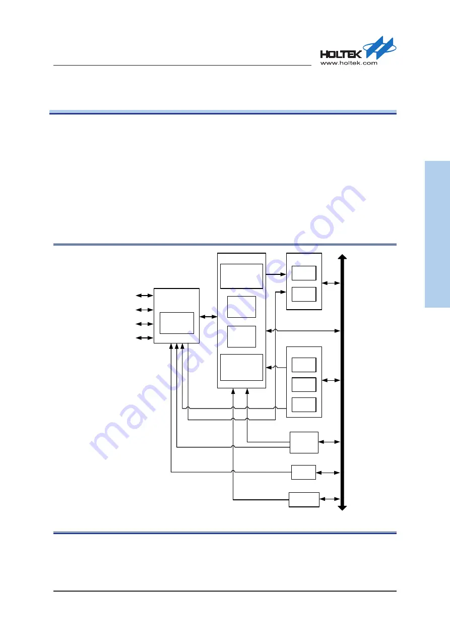
The Serial Peripheral Interface, SPI, provides an SPI protocol data transmit and receive functions
in both master or slave mode. The SPI interface uses 4 pins, among which are the serial data input
and output lines SPI_MISO and SPI_MOSI, the clock line SPI_SCK, and the slave select line
SPI_SEL. One SPI device acts as a master who controls the data flow using the SEL and SCK
signals to indicate the start of the data communication and the data sampling rate. To receive the
data bits, the streamlined data bits which range from 1 bit to 16 bits specified by the DFL field in
the SPICR1 register are latched on a specific clock edge and stored in the data register or in the RX
FIFO. Data transmission is carried out in a similar way but with the reverse sequence. The mode
fault detection provides a capability for multi-master applications.
TXFIFO
RXFIFO
MOSI
MISO
SEL
SCK
SPICR0
SPICR1
SPIFCR
Control
TX Buffer
RX Buffer
SPISR
SPIFSR
SPICPR
SPIFTOCR
Status
APB
Bus
SPIDR
SPIIER
Transmit/Receive
Logic
Shift
Register
Figure 154. SPI Block Diagram