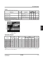


S1F76300 Series
S1F70000 Series
EPSON
4–33
Technical Manual
S1F76300
Series
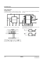
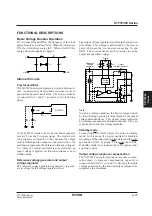
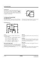
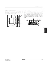
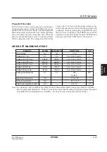
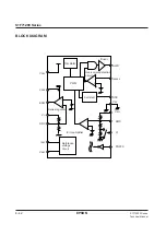
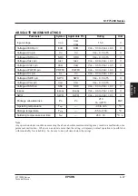
Output voltage adjustment
To ensure stable output, any circuit that adjusts the out-
put voltage must contain C1, R
A
and R
B
. To stop
switching current from affecting V
O
, the circuit must
also satisfy the condition I
O
< I
R
.
The following figure summarizes the relevant circuits
inside an S1F70000 series chip.
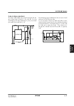
V
O
is connected to the level shift and buffer circuit,
which provide the gate bias for the switching transistor
driving the inductor. The current drain I
O1
, varies with
the load and is typically 10
µ
A. The current, I
O2
,
through the internal resistors R1 and R2 is typically
1
µ
A.
V
I
V
O
I
O
C
L
(I
O
< I
R
)
I
R
R
B
R
A
C
GND
V
SW
Voltage adjustment
circuit
Step-up
voltage
output
SCI7631M/C
V
SW
V
I
Comparator
Controller
Level
shifter
V
O
I
O1
I
O2
V
REF
R1
R2
I
O
Buffer
Summary of Contents for S1F76610C0B0
Page 4: ...S1F70000 Series Technical Manual ...
Page 17: ...1 DC DC Converter ...
Page 43: ...2 DC DC Converter Voltage Regulator ...
Page 107: ...3 Voltage Regulator ...
Page 145: ...4 DC DC Switching Regulators ...
Page 200: ...5 Voltage Detector ...
Page 223: ...6 Appendix ...


