


S1F76540 Series
S1F70000 Series
EPSON
2–19
Technical Manual
S1F76540
Series
ELECTRICAL CHARACTERISTICS
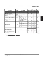
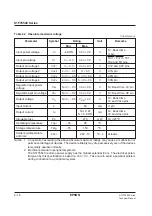
Table 2.3 DC characteristics (1)
Parameter
Symbol
Characteristics
Min.
Typ.
Max. Unit
N = Boost time if CT0 is selected
–22/N
–2.4
V
Input power voltage
V
I
N = Boost time if CT1 is selected
–22/N
–2.4
V
N = Boost time if CT2 is selected
–22/N
–2.4
V
N = Boost time if CT3 is selected
–22/N
–2.4
V
Boost start input power
V
STA
N = Boost time, FC = V
DD
during
–22/N
–2.4
V
voltage
no loading
Boost output voltage
V
O
–22
V
Regulator input voltage
V
RI
–22
–2.4
V
Regulator output voltage
V
REG
I
REG
= 0, V
RI
= –22 V
–2.4
V
R
RV
= 1M
Ω
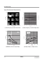
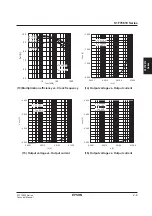
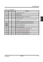
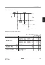
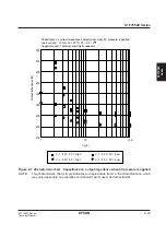
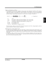
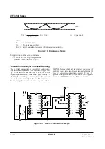
Figure 2.3 Potential relationship
Ta = –30
°
C to +85
°
C, V
DD
= 0 V, V
I
= –5.0 V
unless otherwise noted
V
CC
(+5 V)
GND
(0 V)
V
DD
(0 V)
V
I
(–5 V)
5 V
System
S1F76540
10 V
Two-time
boosting
Three-time
boosting
Four-time
boosting
15 V
20 V
–10 V
–15 V
–20 V
Summary of Contents for S1F76610C0B0
Page 4: ...S1F70000 Series Technical Manual ...
Page 17: ...1 DC DC Converter ...
Page 43: ...2 DC DC Converter Voltage Regulator ...
Page 107: ...3 Voltage Regulator ...
Page 145: ...4 DC DC Switching Regulators ...
Page 200: ...5 Voltage Detector ...
Page 223: ...6 Appendix ...


