


S1F79100Y Series
S1F70000 Series
EPSON
3–35
Technical Manual
S1F79100Y
Series
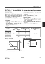
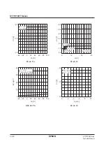
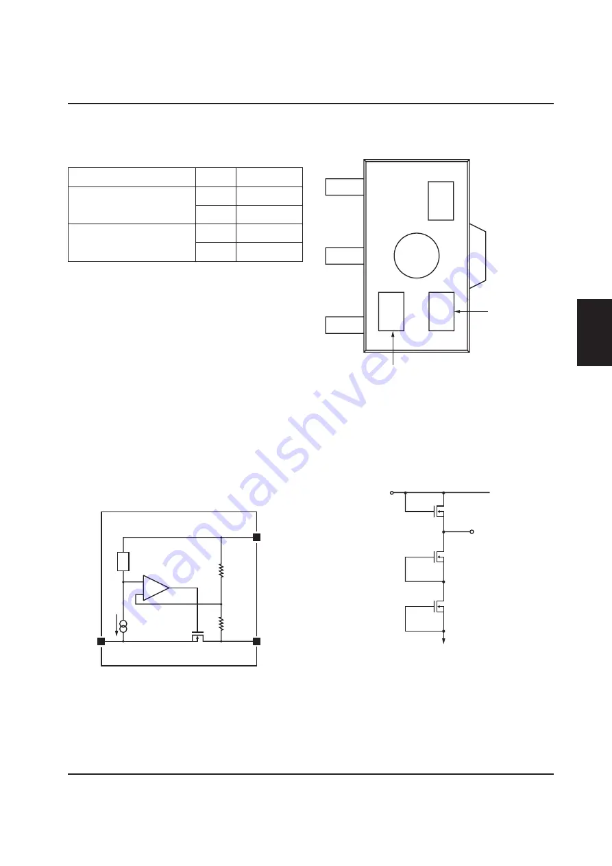
PACKAGE MARKINGS
The markings on S1F79100Y series device packages
use the following abbreviations.
Marking locations
Voltage regulator
code
Output voltage
code
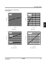
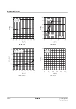
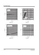
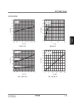
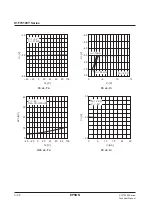
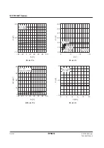
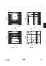
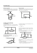
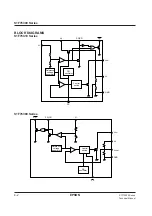
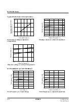
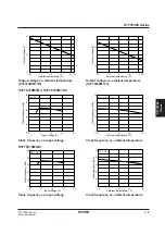
FUNCTIONAL DESCRIPTIONS
Basic Operation
The S1F79100Y series uses a 3-pin series regulator
feedback loop. An operational amplifier compares
V
REG
from the voltage divider formed by R
1
and R
2
,
with V
REF
. The amplifier output adjusts the output
transistor gate bias to equalize the voltages and com-
pensate for fluctuations in V
I
.
V
REF
GND
V
O
R
1
V
REG
R
2
V
I
–
+
The following equation shows the relationship between
V
O
and V
REF
.
R
1
+ R
2
V
O
= ————— V
REF
R
1
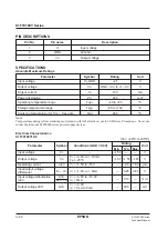
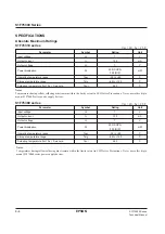
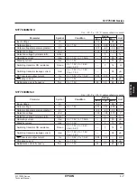
Parameter
Code
Description
Output voltage code
B
5 V
D
3 V
Voltage regulator code
P
Positive
N
Negative
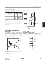
Note
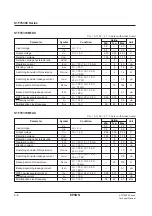
The reflow furnace temperature profile requirements
must be satisfied during package reflow. Avoid solder-
ing on surface mount package (including SOT89) as it
causes a quick temperature change of package and a
device damage.
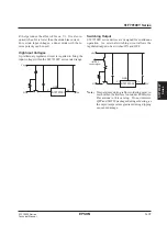
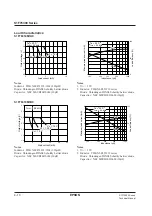
Internal Circuits
Reference voltage generator
The offset structure used in all three transistors results
in a high breakdown voltage that ensures a stable refer-
ence voltage output over a wide range of input voltages.
V
REF
V
1
V
SS
Enhancement
mode
Depletion
mode
Depletion
mode
Summary of Contents for S1F76610C0B0
Page 4: ...S1F70000 Series Technical Manual ...
Page 17: ...1 DC DC Converter ...
Page 43: ...2 DC DC Converter Voltage Regulator ...
Page 107: ...3 Voltage Regulator ...
Page 145: ...4 DC DC Switching Regulators ...
Page 200: ...5 Voltage Detector ...
Page 223: ...6 Appendix ...