


S1F76540 Series
2–22
EPSON
S1F70000 Series
Technical Manual
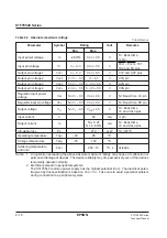
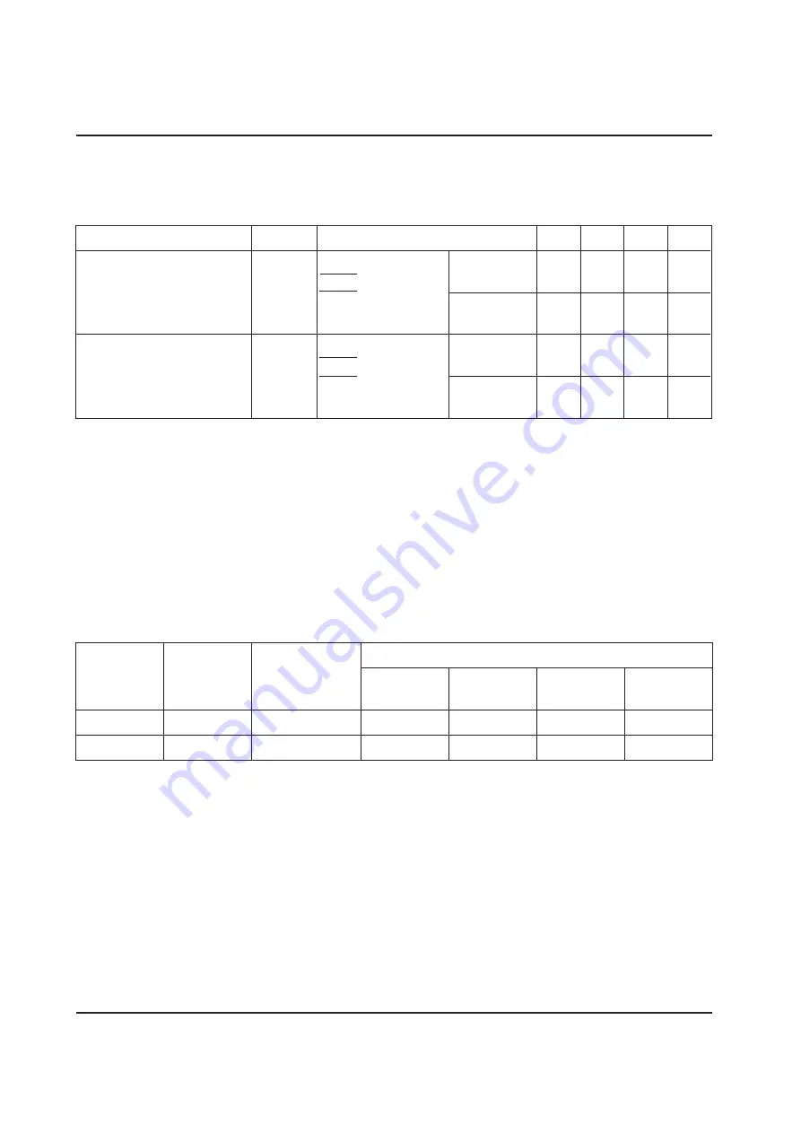
Table 2.4 AC characteristics
V
DD
= 0 V and V
I
= –5.0 V
unless otherwise noted
Parameter
Symbol
Conditions
Min.
Typ.
Max.
Unit
FC = V
DD
,
Ta = 25
°
C
3.0
4.0
6.0
kHz
Internal clock frequency 1
f
CL1
P
OFF1
= V
I
P
OFF2
= V
DD
Ta = –30
°
C
2.0
4.0
7.0
kHz
Pin used: C1P
to +85
°
C
FC = V
I
,
Ta = 25
°
C
12.0
16.0
24.0
kHz
Internal clock frequency 2
f
CL2
P
OFF1
= V
I
P
OFF2
= V
DD
Ta = –30
°
C
8.0
16.0
28.0
kHz
Pin used: C1P
to +85
°
C
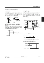
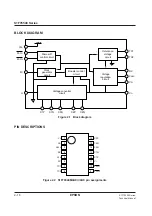
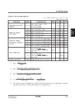
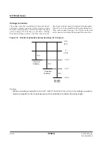
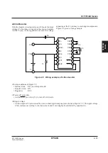
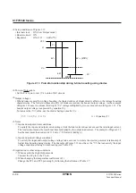
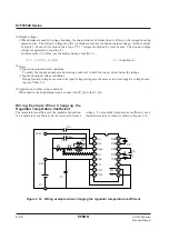
FUNCTIONAL DESCRIPTIONS
Clock Generator Circuit
As the S1F76540 has a built-in clock generator circuit,
no more parts are required for voltage boost control.
The clock frequency changes according to the FC pin
voltage level as defined on Table 2.5. Low Output mode
or High Output mode is selectable. This allows fre-
quency selection according to the used capacitance and
load current as the boost output impedance changes de-
pending on the clock frequency and external booster ca-
pacitance. However, the High Output mode has the
current consumption approximately four times larger
than the Low Output mode.
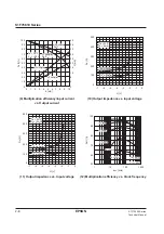
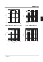
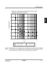
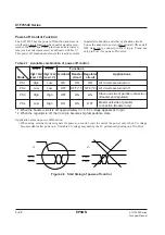
Table 2.5 FC pin setup
Characteristics
FC pin
Mode
Clock frequency
Current
Output ripple
Output
Capacitance
consumption
impedance
High (V
DD
)
Low Output
4.0 kHz (Typ.)
I
OP
(*1)
V
RR
(*2)
See Figure A1. See Figure A1.
Low (V
I
)
High Output
16.0 kHz (Typ.) I
OP
×
Approx. 4 V
RI
×
Approx. 1/4 See Figure A1. See Figure A1.
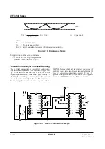
*1 See the DC characteristics table for current consumption.
*2 See Section Page 2-32 for the output ripple definition and calculation.
Summary of Contents for S1F76610C0B0
Page 4: ...S1F70000 Series Technical Manual ...
Page 17: ...1 DC DC Converter ...
Page 43: ...2 DC DC Converter Voltage Regulator ...
Page 107: ...3 Voltage Regulator ...
Page 145: ...4 DC DC Switching Regulators ...
Page 200: ...5 Voltage Detector ...
Page 223: ...6 Appendix ...


