


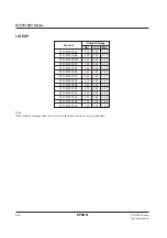


S1F76640 Series
2–60
EPSON
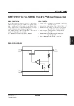
S1F70000 Series
Technical Manual
Negative Voltage Conversion
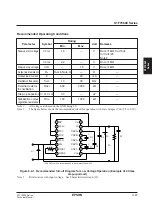
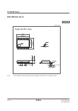
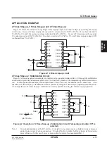
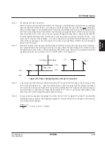
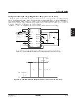
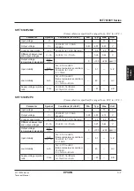
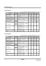
S1F76640 can boost input voltage to negative power on the negative potential side by using the circuit shown in
Figure 8.6. (In case of 3 times step-up, remove the capacitor C
3
and the diode D
4
and short-circuit the both ends of
D
4
. In case of 2 times step-up, remove the capacitor C
2
and the diode D
3
and short-circuit the both ends of D
3
.) But
the output voltage drops by the forward voltage V
F
of the diode. When GND is 0V, V
DD
is 5V and VF is 0.6V as
shown in Figure 8.6 for example, V
O
is calculated as follows: V
O
= –15V–4
×
0.6V = –12.6V(In case of 3 times
step-up, V
O
is calculated to –10V–3
×
0.6V = –8.2V, and in case of 2 times step-up, V
O
is calculated to –5V–2
×
0.6V
= –3.8V.)
Figure 8.6 Negative Voltage Conversion (Example of 3 times step-up circuit)
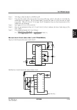
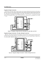
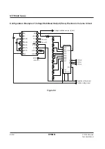
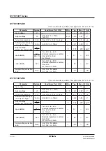
Negative Voltage Conv Positive Voltage Conversion
When the 3 times step-up operation shown in Figure 8.1 and the positive voltage conversion in Figure 8.6 are
combined, the circuit shown in Figure 8.7 can be formed and 20V and –12.6V can be obtained from the input 5V.
However, the output impedance is higher than in case of connection of either one only (the negative voltage conver-
sion or the positive voltage conversion).
Figure 8.7 Negative Voltage Conv Positive Voltage Conversion
RV
V
REG
TC1
TC2
P
OFF
V
SS
OSC1
OSC2
1
2
3
4
5
6
7
8
16
15
14
13
12
11
10
9
V
RI
V
O
CAP3+
CAP2+
CAP2–
CAP1+
CAP1–
V
DD
D
3
D
2
D
1
V
O
'
C
0
C
1
C
2
+
+
–
+
–
–
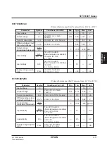
RV
V
REG
TC1
TC2
P
OFF
V
SS
OSC1
OSC2
1
2
3
4
5
6
7
8
16
15
14
13
12
11
10
9
V
RI
V
O
CAP3+
CAP2+
CAP2–
CAP1+
CAP1–
V
DD
V
O
'
V
O
'
+
–
+
+
–
+
–
+
–
–
+
–
Summary of Contents for S1F76610C0B0
Page 4: ...S1F70000 Series Technical Manual ...
Page 17: ...1 DC DC Converter ...
Page 43: ...2 DC DC Converter Voltage Regulator ...
Page 107: ...3 Voltage Regulator ...
Page 145: ...4 DC DC Switching Regulators ...
Page 200: ...5 Voltage Detector ...
Page 223: ...6 Appendix ...