


S1F76640 Series
S1F70000 Series
EPSON
2–43
Technical Manual
S1F76640
Series
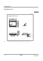
FUNCTIONAL DESCRIPTIONS
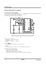
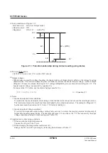
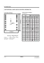
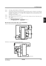
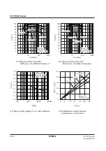
CR Oscillator
S1F76640 has a built-in CR oscillator as the internal oscillator, and an external oscillation resistor R
OSC
is
connected between the pins OSC1 and OSC2 before operation. (Figure 5.1)
Figure 5-1 CR Oscillator
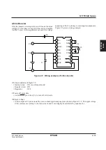
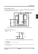
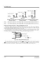
Figure 5-2 External Clock Operation
Note 1 :
Since the oscillation frequency varies with wiring capacitance, make the cables between the terminals
OSC1 and OSC2 and R
OSC
as short as possible.
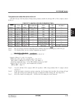
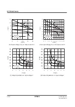
When setting the external resistor R
OSC
, find the oscillation frequency f
OSC
that brings about the maximum effi-
ciency from Figures 6.5.12 and 6.5.13 and find R
OSC
suitable for the f
OSC
from Figure 6.5.1 The relations between
R
OSC
and f
OSC
in Figure 6.5.1 are expressed approximately with the following formula as far as the straight portion
(500k
Ω
< R
OSC
< 2M
Ω
) is concerned:
R
OSC
= A
⋅
1
f
OSC
So, the R
OSC
value can be obtained from this formula.
(Recommended oscillation frequency : 10kHz to 30kHz (R
OSC
: 2M
Ω
to 680k
Ω
)
When the external clock operates, make the pin OSC2 open as shown in Figure 5.2 and input the 50% duty of the
external clock from the pin OSC1.
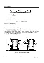
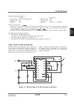
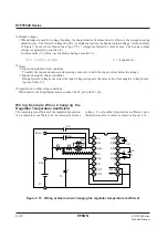
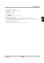
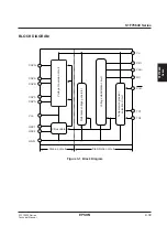
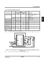
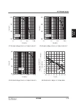
Voltage Conversion Circuits (I) and (II)
The voltage conversion circuits (I) and (II) doubles and triples the input voltage V
DD
respectively by using clock
generated in the CR oscillator.
In case of 2 times step-up, 2 times step-up output of the input voltage is obtained from the V
O
pin when a pump up
capacitor is connected between CAP1+ and CAP1–, CAP2+ and CAP3+ are short-circuited to V
O
and a smoothing
capacitor is connected between V
DD
and V
O
outside.
In case of 3 times step-up, 3 V
DD
is output from the V
O
pin when a pump up capacitor is connected between
CAP1+ and CAP1– and between CAP2+ and CAP2– respectively and a smoothing capacitor is connected between
the V
DD
and V
O
pins outside.
In case of 4 times step-up, 4 V
DD
is output from the V
O
pin when a pump up capacitor is connected between
CAP1+ and CAP1–, between CAP2+ and CAP2– and between CAP1+ and CAP3– respectively and a smoothing
capacitor is connected between the V
DD
and V
O
pins outside.
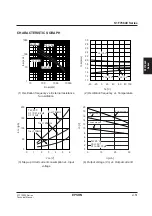
When GND is 0 and V
DD
is 5, the relations between the input voltage and the output voltage are as shown in
Figures 5-3, 5-4 and 5-5.
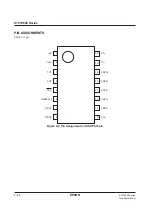
OSC1
OSC2
OSC1
OSC2
Open
External clock
(Note 1)
R
OSC
A : Constant, When GND is 0V and
V
DD
is 5V, A is 2.0
×
10
10
(1/F).)
[ ]
Summary of Contents for S1F76610C0B0
Page 4: ...S1F70000 Series Technical Manual ...
Page 17: ...1 DC DC Converter ...
Page 43: ...2 DC DC Converter Voltage Regulator ...
Page 107: ...3 Voltage Regulator ...
Page 145: ...4 DC DC Switching Regulators ...
Page 200: ...5 Voltage Detector ...
Page 223: ...6 Appendix ...


