


S1F71200 Series
4–44
EPSON
S1F70000 Series
Technical Manual
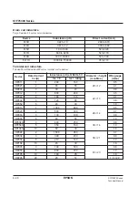
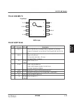
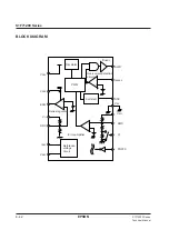
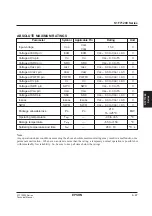
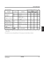
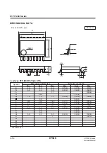
PIN DESCRIPTIONS
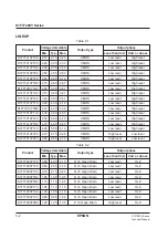
Pin No.
1
2
3
4
5
6
7
8
9
10
11
12
13
14
15
16
Pin name
V
DD1
V
DD2
EXO
V
O
SRC
I
REF
V
REF
(N.C)
POFFX
V
C
SWC
V
SW
V
SS
SSC
I
SENSE
SWO
Pin type
Power supply
Power supply
Output
—
—
Output
Output
—
Input
Input
—
—
—
—
Input
Output
Power system
V
DD1
V
DD2
V
DD2
—
—
V
DD1
V
DD1
—
V
DD1
V
DD1
—
—
—
V
DD1
V
DD1
V
DD1
Description
Power pin 1 (+), Input power pin
Power pin 2 (+), Power pin for series regulator
circuit
PNP transistor base drive pin for series regulator
Step-up/step-down output feedback pin
Series regulator phase compensation capaci-
tor connection pin
Reference resistor connection pin. Connect a
100k
Ω
resistor between the V
SS
pins.
Reference voltage pin. Connect a 0.1
µ
F
capacitance between the V
SS
pins.
No connection
Power off control pin.
During normal operation : POFFX = V
DD1
At power off time
: POFFX = V
SS
Step-up output voltage setting pin.
For setting V
SW
= V
O
+ 1.0V : V
C
= V
DD1
For setting V
SW
= V
O
+ 0.5V : V
C
= V
SS
Switching regulator phase compensation
capacitor connection pin
Step-up output feedback pin
Power pin (–), Ground pin
Capacitor connection pin for soft start
Overcurrent detection pin
Step-up switching power transistor drive pin
Summary of Contents for S1F76610C0B0
Page 4: ...S1F70000 Series Technical Manual ...
Page 17: ...1 DC DC Converter ...
Page 43: ...2 DC DC Converter Voltage Regulator ...
Page 107: ...3 Voltage Regulator ...
Page 145: ...4 DC DC Switching Regulators ...
Page 200: ...5 Voltage Detector ...
Page 223: ...6 Appendix ...


