


S1F76600 Series
1–2
EPSON
S1F70000 Series
Technical Manual
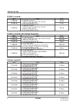
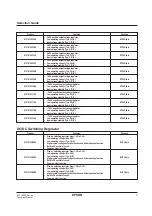
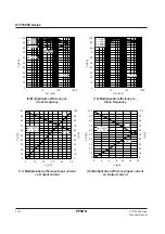
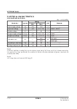
Parameter
Symbol
Rating
Unit
Input voltage range
V
I
–10.0 to 0.5
V
Output voltage range
V
O
Min. –20.0
V
Power dissipation
P
D
300 (DIP)
mW
150 (SOP)
Operating temperature range
T
opr
–40 to +85
˚C
Storage temperature range
T
stg
–65 to +150
˚C
Soldering temperature(for 10s). See note.
T
sol
260
˚C
SPECIFICATIONS
Absolute Maximum Ratings
Note:
Temperatures during reflow soldering must remain within the limits set out in LSI Device Precautions.
Never use solder dip to mount S1F70000 series power supply devices.
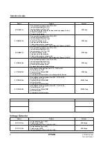
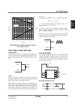
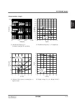
Recommended Operating Conditions
V
DD
= 0V, Ta = –40 to +85˚C unless otherwise noted
Parameter
Symbol
Condition
Rating
Unit
Min.
Typ.
Max.
R
OSC
= 1M
Ω
,
C
1
/C
2
≤
1/20, C
2
≥
10
µ
F,
—
—
–1.5
Oscillator startup voltage
V
STA
Ta = –20 to +85˚C
V
See note 1.
R
OSC
= 1M
Ω
—
—
–2.2
Oscillator shutdown voltage
V
STP
R
OSC
= 1M
Ω
–1.5
—
—
V
Load resistance
R
L
R
L
min
—
—
Ω
See note 2.
Output current
I
O
—
—
30.0
mA
Clock frequency
f
OSC
10.0
—
30.0
kHz
CR oscillator network
R
OSC
680
—
2,000
k
Ω
resistance
Capacitance
C
1
, C
2
3.3
—
—
µ
F
Notes:
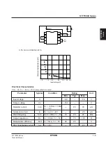
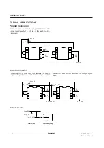
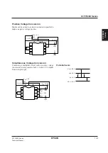
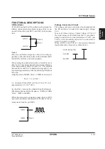
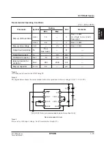
1. The recommended circuit configuration for low-voltage operation (when V
I
is between –1.2V and
–2.2V) is shown in the following figure. Note that diode D1 should have a maximum forward voltage of
0.6V with 1.0mA forward current.
2. R
L
min can be varied depending on the input voltage.
Summary of Contents for S1F76610C0B0
Page 4: ...S1F70000 Series Technical Manual ...
Page 17: ...1 DC DC Converter ...
Page 43: ...2 DC DC Converter Voltage Regulator ...
Page 107: ...3 Voltage Regulator ...
Page 145: ...4 DC DC Switching Regulators ...
Page 200: ...5 Voltage Detector ...
Page 223: ...6 Appendix ...


