

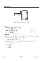
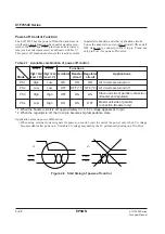

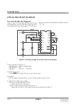

S1F76540 Series
2–18
EPSON
S1F70000 Series
Technical Manual
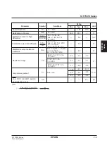
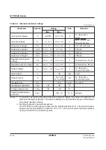
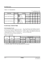
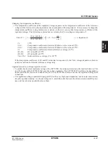
Table 2.2 Absolute maximum ratings
V
DD
reference
Parameter
Symbol
Rating
Unit
Remarks
Min.
Max.
Input power voltage
V
I
–26.0/N
V
DD
+ 0.3
V
N = Boost time
V
I
pin
Input pin voltage
V
1
V
I
– 0.3
V
DD
+ 0.3
V
P
OFF1
, P
OFF2
, TC1,
TC2 and FC pins
Output pin voltage 1
V
OC1
V
I
–
0.3
V
DD
+
0.3
V
C1P and C2P pins
Output pin voltage 2
V
OC2
2
×
V
I
–
0.3
V
I
+
0.3
V
C1N pin
Output pin voltage 3
V
OC3
3
×
V
I
– 0.3
2
×
V
I
+ 0.3
V
C2N pin
Output pin voltage 4
V
OC4
4
×
V
I
– 0.3
3
×
V
I
+ 0.3
V
C3N pin
Regulator input power
V
RI
N
×
V
I
– 0.3
V
DD
+ 0.3
V
N = Boost time, V
RI
pin
voltage
Regulator input pin voltage
V
RV
N
×
V
I
– 0.3
V
DD
+ 0.3
V
N = Boost time, RV pin
Output voltage
V
O
N
×
V
I
– 0.3
V
DD
+ 0.3
V
N = Boost time
V
O
and V
REG
pins
Input current
I
I
80
mA
V
I
pin
Output current
I
O
N
≤
4: 20
mA
N = Boost time
N > 4: 80/N
V
O
and V
REG
pins
Allowable loss
P
D
210
mW
Ta
≤
25
°
C
Operating temperature
Topr
–30
85
°
C
Storage temperature
Tstg
–55
150
°
C
Soldering temperature
Tsol
260
•
10
°
C
•
s
At leads
and time
Notes: 1. An operation exceeding the above absolute maximum ratings may cause a malfunction or
permanent damage of devices. The device reliability may drop excessively even if the devices
temporarily operate normally.
2. Electrical potential to peripheral systems:
The S1F76540 common power supply has the highest potential (V
DD
). The electrical poten-
tial given by this specification is based on V
DD
= 0 V. Take care to avoid a potential problem
during connection to a peripheral system.
Summary of Contents for S1F76610C0B0
Page 4: ...S1F70000 Series Technical Manual ...
Page 17: ...1 DC DC Converter ...
Page 43: ...2 DC DC Converter Voltage Regulator ...
Page 107: ...3 Voltage Regulator ...
Page 145: ...4 DC DC Switching Regulators ...
Page 200: ...5 Voltage Detector ...
Page 223: ...6 Appendix ...