


S1F76640 Series
S1F70000 Series
EPSON
2–57
Technical Manual
S1F76640
Series
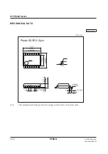
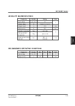
APPLICATION EXAMPLE
2 Times Step-up, 3 Times Step-up and 4 Times Step-up
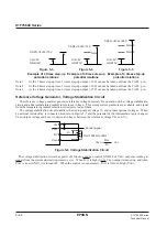
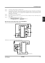
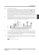
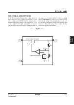
Figure 8.1 shows the connection for getting 4 times step-up output of an input voltage by operating the step-up
circuit only. In case of 3 times step-up, the capacitor C
3
is removed and CAP3+ (Pin No. 14) is short-circuited to
V
O
(Pin No. 15), and 3 times step-up voltage is obtained from V
O
(CAP3+). In case of 2 times step-up, the capacitor
C
2
is also removed and CAP2+ (Pin No. 13) is short-circuited to V
O
(Pin No. 15), and 2 times step-up voltage (10V)
is obtained from V
O
(CAP2+).
Figure 8-1 4 times step-up circuit
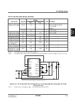
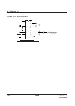
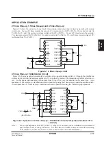
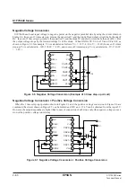
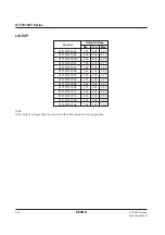
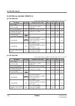
4 Times Step-up + Stabilization Circuit
Figure 8-2 shows an application example for stabilizing step-up outputs obtained in 8-(1) through the stabilization
circuit and for providing temperature gradient to V
REG
output by means of the temperature gradient selection cir-
cuit. In this application example, both outputs from V
O
and V
REG
can be indicated at the same time. Also,
operation of 3 times step-up + stabilization circuit is possible by using the 3 times step-up operation mentioned in 8-
(1), and operation of 2 times step-up + stabilization circuit is possible by using the 2 times step-up operation.
Figure 8-2 Operation of 4 Times Step-up + Stabilization Circuit (Temperature Gradient CT1 is
selected.)
Note 1 :
Since input impedance at the RV pin (No. 1) is high, it is necessary to use a shielded wire as a measure
against noise in case of a long connection. It is also effective to make the R
RV
value small for reducing
noise influence. (In this case, however, more current comes to be consumed at R
RV
.)
C
1
V
I
C
2
C
3
C
4
4V
I
+
–
+
–
+
–
+
–
RV
V
REG
TC1
TC2
P
OFF
V
SS
OSC1
OSC2
1
2
3
4
5
6
7
8
16
15
14
13
12
11
10
9
V
RI
V
O
CAP3+
CAP2+
CAP2–
CAP1+
CAP1–
V
DD
RV
V
REG
TC1
TC2
P
OFF
V
SS
OSC1
OSC2
1
2
3
4
5
6
7
8
16
15
14
13
12
11
10
9
V
RI
V
O
CAP3+
CAP2+
CAP2–
CAP1+
CAP1–
V
DD
C
2
C
5
+
–
C
1
+
–
C
3
+
–
C
4
V
I
R
1
R
1
R
1
+R
2
R
2
+
–
+
–
Note 1
V
REG
= ·V
RV
V
REG
(R
RV
=R
1
+R
2
)
Note 2
Summary of Contents for S1F76610C0B0
Page 4: ...S1F70000 Series Technical Manual ...
Page 17: ...1 DC DC Converter ...
Page 43: ...2 DC DC Converter Voltage Regulator ...
Page 107: ...3 Voltage Regulator ...
Page 145: ...4 DC DC Switching Regulators ...
Page 200: ...5 Voltage Detector ...
Page 223: ...6 Appendix ...