


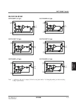
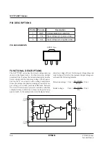


S1F70000 Series
EPSON
5–5
Technical Manual
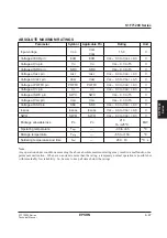
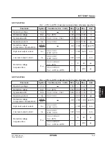
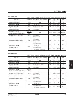
S1F77200Y Series
S1F77200Y
Series
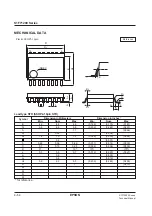
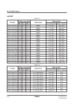
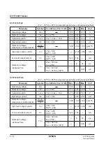
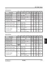
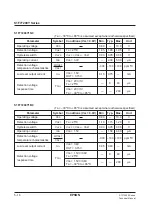
The following figures show the input and output characteristics of the S1F77200Y series.
[S1F772
*
0Y1
*
0 Type]
S1F772
*
0Y2
*
0 Type
Note:
The above input/output characteristics assumes that the pull up resistor is connected to the output pin for
the S1F77200Y series. For the S1F77220 series, it assumes that the pull down resistor is connected
between the OUT and V
DD
pins.
If the input voltage that is applied between V
DD
and V
SS
terminals drops below the lower limit of voltage
for IC operation, the output condition of the OUT terminal may become unsteady.
Ensure to prevent problems from occurring in circuit operation.
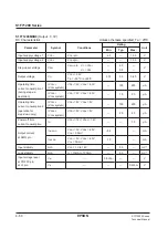
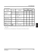
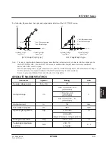
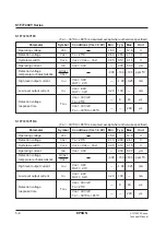
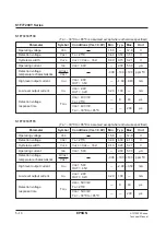
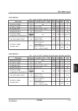
ABSOLUTE MAXIMUM RATINGS
OUT
0
0
V
DD
(V1)
V
HYS
V
DET
: Detection voltage
V
REL
: Relief voltage
V
REL
V
DET
Operating voltage
upper limit
Operating voltage
lower limit
OUT
0
0
V
DD
(V1)
V
HYS
V
DET
: Detection voltage
V
REL
: Relief voltage
V
REL
V
DET
Operating voltage
upper limit
Operating voltage
lower limit
Parameter
Symbol
Rating
Unit
Supply voltage range
V
DD
– V
SS
15
V
V
DD
+ 0.3 to V
SS
– 0.3
(S1F77210)
Output voltage
V
O
15 to V
SS
– 0.3
V
(S1F77200)
V
DD
+ 0.3 to V
DD
– 15
(S1F77220)
Output current
I
O
50
mA
Allowable dissipation
P
D
200
mW
Operating temperature
Topr
–40 to +85
°
C
–30 to +85
(designed for lower voltage operation)
Storage temperature
Tstg
–65 to +150
˚C
Soldering temperature
Tsol
260 · 10
˚C · s
and time
(at leads)
Summary of Contents for S1F76610C0B0
Page 4: ...S1F70000 Series Technical Manual ...
Page 17: ...1 DC DC Converter ...
Page 43: ...2 DC DC Converter Voltage Regulator ...
Page 107: ...3 Voltage Regulator ...
Page 145: ...4 DC DC Switching Regulators ...
Page 200: ...5 Voltage Detector ...
Page 223: ...6 Appendix ...