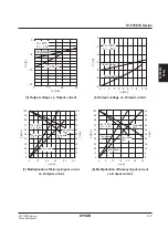
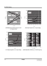
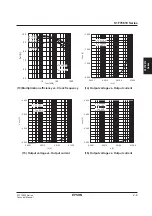


S1F76540 Series
S1F70000 Series
EPSON
2–17
Technical Manual
S1F76540
Series
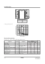
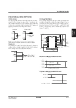
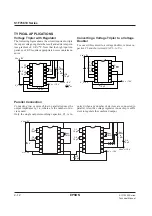
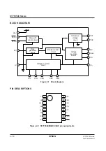
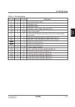
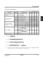
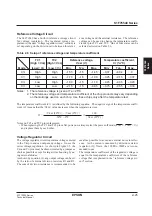
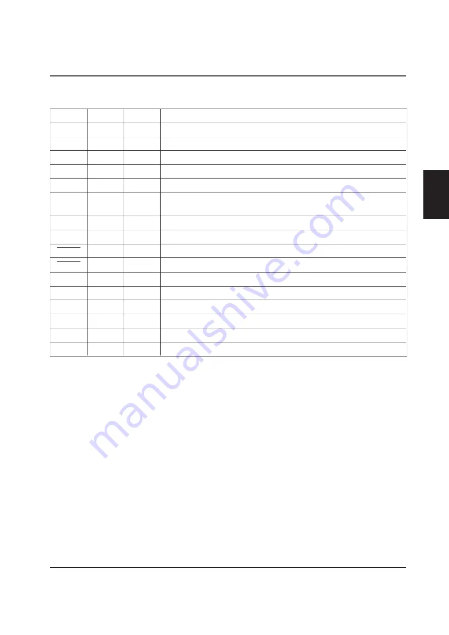
Table 2.1 Pin descriptions
Pin name Pin No.
Pad No.
Description
V
O
1
18
Four-time booster output
V
RI
2
19
Regulator input
V
REG
3
20
Regulator output
R
V
4
21
Regulator output voltage adjustment input
V
DD
5
22, 23
Power pin (positive)
FC
6
24
Internal clock frequency input, and clock input in serial/parallel
connection
TC1
7
3
Regulator output temperature gradient setup input (1)
TC2
8
4
Regulator output temperature gradient setup input (2)
P
OFF2
9
5
Power-off control input (2)
P
OFF1
10
6
Power-off control input (1)
V
I
11
11, 12
Power voltage (negative)
C1P
12
13
Two- or four-time booster capacitor positive pin
C1N
13
14
Two-time booster capacitor negative pin
C3N
14
15
Four-time booster capacitor negative pin
C2N
15
16
Three-time booster capacitor negative pin
C2P
16
17
Three-time booster capacitor positive pin
Summary of Contents for S1F76610C0B0
Page 4: ...S1F70000 Series Technical Manual ...
Page 17: ...1 DC DC Converter ...
Page 43: ...2 DC DC Converter Voltage Regulator ...
Page 107: ...3 Voltage Regulator ...
Page 145: ...4 DC DC Switching Regulators ...
Page 200: ...5 Voltage Detector ...
Page 223: ...6 Appendix ...


