


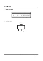

S1F76640 Series
S1F70000 Series
EPSON
2–59
Technical Manual
S1F76640
Series
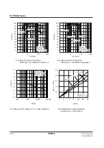
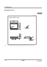
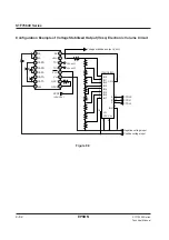
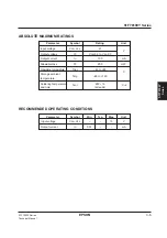
Note 1 :
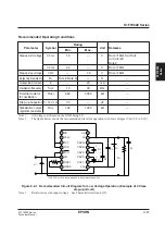
Precautions on Load Connection
When a load is connected between GND in the first stage (or potential below GND in the second stage
other than that) and V
REG
in the second stage as shown in Figure 8.4, pay attention to the following.
When a normal output is not available at the V
REG
pin at the starting time or when the P
OFF
signal turns
off V
REG
, current may flows from GND in the first stage (or potential below GND in the second stage
other than that) to the V
REG
pin in the second stage through the load and a voltage higher than the
absolute maximum rating below GND in the second stage may be generated at the V
REG
pin. As a
result, the IC may not work normally. For series connection, connect the diode D1 between V
DD
and
V
REG
in the second stage as shown in Figure 8.4, so that no potential below GND in the second stage is
added to the V
REG
pin.
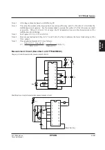
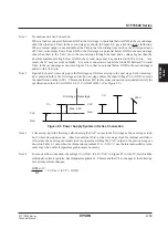
Note 2 :
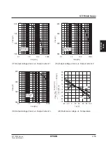
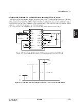
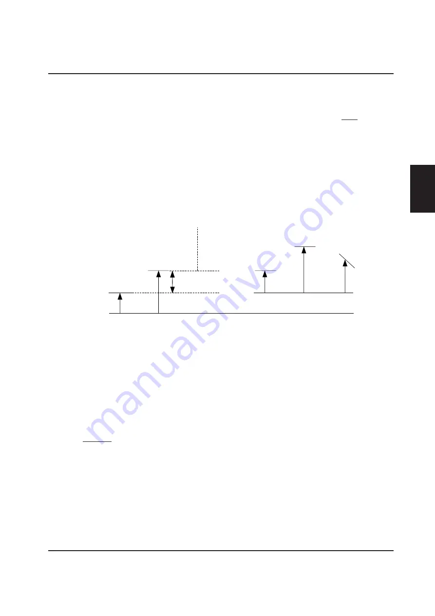
Figure 8.4 shows 3 times step-up in the first stage and 4 times step-up in the next stage, but 4 times step-
up is possible both in the first stage and in the next stage unless the input voltage V
DD
’-GND’ exceeds
the specification value (6.0V). This means that each IC in this series connection is requested t satisfy the
specification values (V
DD
-GND
≤
6, 0V, V
O
-GND
≤
24V). (See Figure 8.5.)
Figure 8.5 Power Supply System in Series Connection
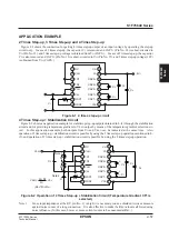
Note 3 :
2 times step-up in the first stage allows using the CAP- output in the first stage as the next stage clock,
but 3 times step-up does not. Attach an external R
OSC
as the next stage clock for internal oscillation.
Also, since the next stage external clock can operate according the CAP- output in the previous stage as
shown in Table 4.1 only when the temperature gradient C
T
is -0.6%/˚C, use the internal oscillator in the
same way when other temperature gradients are necessary.
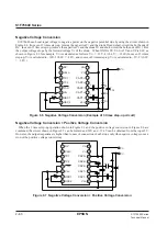
Note 4 :
In case of series connection, the voltage V
DD
-V
REG
(V
REG
’-V
DD
’ in Figure 8.5) of the IC, for which the
stabilization circuit operates, has temperature gradient. This means that V
REG
changes at the following
rate as temperature changes:
∆
V
REG
= C
T
(V
REG
’ (25˚C) – GND’)
∆
T
V
DD
G
ND
V
O
Max. 6.0V
V
DD
'
G
ND
'
V
O
'
V
REG
'
First stage
Next stage
Summary of Contents for S1F76610C0B0
Page 4: ...S1F70000 Series Technical Manual ...
Page 17: ...1 DC DC Converter ...
Page 43: ...2 DC DC Converter Voltage Regulator ...
Page 107: ...3 Voltage Regulator ...
Page 145: ...4 DC DC Switching Regulators ...
Page 200: ...5 Voltage Detector ...
Page 223: ...6 Appendix ...


