14 Servicing & Parts Replacement
47
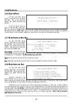
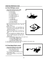
14.3 Main PCB Replacement
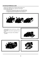
1. Follow all of the directions in section 14.2 first.
2. Unplug the main PCB connectors at:
A. J9, CAL Switch.
B. J10, Peel Sensor.
C. J11, Peel Emitter.
D. J13, Thermal print head.
E. J14, Stepper motor.
F. J15, Gap sensor assembly.
G. J16, Pick-up motor.
H. J17, Display (A).
I. J18, Display (B).
J. J19, Power supply (A).
K. J20, Power supply (B).
L. J21, Load cell data.
M. J22, Load cell power.
3. Remove main post and 5 screws from the main PCB.
4. Slide main PCB upwards so as to clear the
plastic column.
5. Insert new main PCB.
6. Make sure to remove and troubleshoot any
accessories from the old main PCB. These may
include the Memory Expansion PCB or the
Network Memory PCB.
7. After you are sure that these accessories are in
working order, attach them to the new main
PCB.
8. If the new main PCB has no EPROMs, make sure
to use the EPROMs from the old main PCB only
after you have determined that they are in
working order.
9. The main PCB EPROMs are listed below in left-to-right order:
A. U5, Scale System EPROM, 4M bit.
B. U6, Scale Display EPROM, 4M bit.
C. U7, Printer Fonts EPROM, 4M bit .
D. U8, Printer System EPROM, 2M bit.
10. Once EPROMs and accessories are replaced, reassemble scale (reverse order.)
11. Do a Memory All Clear, (see section 8.6)
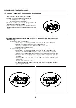
14.4 Power Supply Replacement
1. Follow all of the directions in section 14.2 first.
2. Unplug the Power Supply connectors at:
A. CN1, Input power source.
B. CN21, Output power (A).
C. CN22, Output power (B).
3. Then, remove the 4 screws holding down the
Power Supply chassis.
4. Install new Power Supply and reassemble in
reverse order.
Summary of Contents for LP-2G
Page 2: ......
Page 8: ......
Page 11: ...1 General 3 Note Specifications are subject to change without notice ...
Page 46: ...11 Network Options 38 11 Network Options Refer to Network manual ...
Page 66: ...16 Troubleshooting 58 16 2 Versioning Changes ...
Page 69: ...17 Schematic Diagrams 61 17 3 Main PCB ...
Page 70: ...17 Schematic Diagrams 62 17 4 Ethernet Memory Expansion PCB ...
Page 71: ...17 Schematic Diagrams 63 17 5 Power Supply PCB ...
Page 72: ...18 Exploded Views 64 18 Exploded Views 18 1 Scale ...
Page 73: ...18 Exploded Views 65 18 2 Printer Assembly ...
Page 74: ......
Page 89: ...Appendix C 85 ...
Page 90: ...Appendix C 86 ...
Page 91: ...Appendix C 87 ...
Page 92: ...Appendix C 88 ...
Page 93: ...Appendix C 89 ...
Page 94: ...Appendix C 90 ...
Page 95: ...Appendix C 91 ...
Page 96: ...Appendix C 92 ...
Page 97: ...Appendix C 93 ...
Page 98: ...Appendix C 94 ...
Page 99: ...Appendix C 95 ...
Page 100: ...Appendix C 96 ...
Page 101: ...Appendix C 97 ...
Page 102: ...Appendix C 98 ...
Page 103: ...Appendix C 99 ...
Page 104: ...Appendix C 100 ...

