21
AT94KAL Series FPSLIC
Rev. 1138G–FPSLI–11/03
FPGA/AVR Interface and System Control
The FPGA and AVR share a flexible interface which allows for many methods of system
integration.
•
Both FPGA and AVR share access to the 15 ns dual-port SRAM.
•
The AVR data bus interfaces directly into the FPGA busing resources, effectively treating
the FPGA as a large I/O device. Users have complete flexibility on the types of additional
peripherals which are placed and routed inside the FPGA user logic.
•
Up to 16 decoded address lines are provided into the FPGA.
•
Up to 16 interrupts are available from the FPGA to the AVR.
•
The AVR can reprogram the FPGA during operation to create a dynamic reconfigurable
system (Cache Logic).
FPGA/AVR
Interface–
Memory-mapped
Peripherals
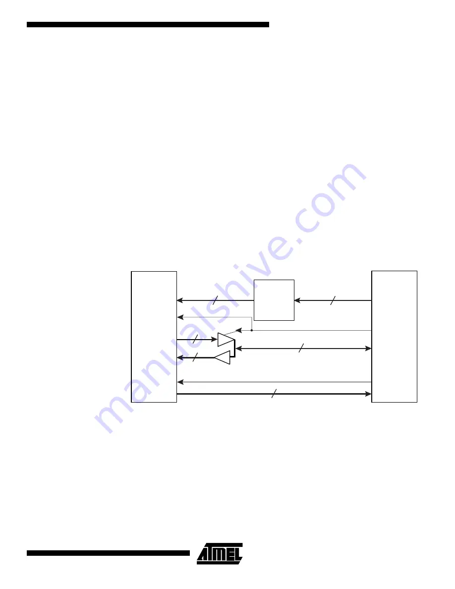
The FPGA core can be directly accessed by the AVR core, see Figure 18. Four memory loca-
tions in the AVR memory map are decoded into 16 select lines (8 for AT94K05) and are
presented to the FPGA along with the AVR 8-bit data bus. The FPGA can be used to create
additional custom peripherals for the AVR microcontroller through this interface. In addition
there are 16 interrupt lines (8 for AT94K05) from the FPGA back into the AVR interrupt control-
ler. Programmable peripherals or regular logic can use these interrupt lines. Full support for
programmable peripherals is available within the System Designer tool suite.
Figure 18.
FPGA/AVR Interface: Interrupts and Addressing
The FPGA I/O selection is controlled by the AVR. This is described in detail beginning on
page 53. The FPGA I/O interrupts are described beginning on page 57.
EMBEDDED
FPGA CORE
EMBEDDED
AVR CORE
ADDRESS
DECODER
4:16
DECODE
Up to 16 Memory-mapped
Decoded Address
Lines from 4 I/O Memory
Space Addresses
I/O Memory Address Bus
FPGAIORE
FPGAIOWE
Up to 16 Interrupt Lines from FPGA to AVR – Various Priority Levels
8-bit Bi-directional Data Bus
8-bit
Data Out
8-bit
Data In


