background image

186

4317I–AVR–01/08

AT90PWM2/3/2B/3B

chronous, Master synchronous and Slave synchronous mode. The UMSEL bit in USART
Control and Status Register C (UCSRC) selects between asynchronous and synchronous oper-
ation. Double Speed (asynchronous mode only) is controlled by the U2X found in the UCSRA
Register. When using synchronous mode (UMSEL = 1), the Data Direction Register for the XCK
pin (DDR_XCK) controls whether the clock source is internal (Master mode) or external (Slave
mode). The XCK pin is only active when using synchronous mode.

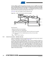
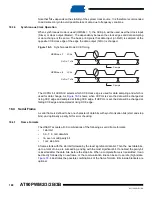
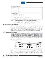
Figure 18-2

 shows a block diagram of the clock generation logic.

Figure 18-2. USART Clock Generation Logic, Block Diagram

Signal description:

txn clk Transmitter clock (Internal Signal).

rxn clk Receiver base clock (Internal Signal).

xn cki Input from XCK pin (internal Signal). Used for synchronous slave operation.

xn cko Clock output to XCK pin (Internal Signal). Used for synchronous master

operation.

f

clk

io

System I/O Clock frequency.

18.3.1

Internal Clock Generation – Baud Rate Generator

Internal clock generation is used for the asynchronous and the synchronous master modes of
operation. The description in this section refers to 

Figure 18-2

.

The USART Baud Rate Register (UBRR) and the down-counter connected to it function as a
programmable prescaler or baud rate generator. The down-counter, running at system clock
(

f

clk

io

), is loaded with the UBRR value each time the counter has counted down to zero or when

the UBRRL Register is written. A clock is generated each time the counter reaches zero. This
clock is the baud rate generator clock output (= 

f

clk

io

/(UBRR+1)). The Transmitter divides the

baud rate generator clock output by 2, 8 or 16 depending on mode. The baud rate generator out-
put is used directly by the Receiver’s clock and data recovery units. However, the recovery units
use a state machine that uses 2, 8 or 16 states depending on mode set by the state of the
UMSEL, U2X and DDR_XCK bits.

Prescaling

Down-Counter

/2

UBRRn

/4

/2

f

clk

UBRRn+1

Sync

Register

clk

XCKn

Pin

txn clk

U2Xn

UMSELn

DDR_XCKn

0

1

0

1

xn cki

xn cko

DDR_XCKn

rxn clk

0

1

1

0

Edge

Detector

UCPOLn

io

io

Summary of Contents for AT90PWM2

Page 1: ...Synchronous Update of all PWM Registers Auto Stop Function for Event Driven PFC Implementation Less than 25 Hz Step Width at 150 kHz Output Frequency PSC2 with four Output Pins and Output Matrix One...

Page 2: ...Compar Application AT90PWM2 AT90PWM2B SO24 2 x 2 8 1 2 One fluorescent ballast AT90PWM3 AT90PWM3B SO32 QFN32 3 x 2 11 2 3 HID ballast fluorescent ballast Motor control Product Revision AT90PWM2 AT90P...

Page 3: ...PB3 AMP0 AREF GND AVCC PB2 ADC5 INT1 PD7 ACMP0 PD6 ADC3 ACMPM INT0 PD5 ADC2 ACMP2 AT90PWM3 3B SOIC 32 1 2 3 4 5 6 7 8 9 10 11 12 13 14 15 16 32 31 30 29 28 27 26 25 24 23 22 21 20 19 18 17 PSCOUT00 X...

Page 4: ...26 25 9 10 11 12 13 14 15 16 MOSI PSCOUT21 PB1 OC0B XTAL1 PE1 ADC0 XTAL2 PE2 ADC1 RXD DALI ICP1_A SCK_A PD4 ADC2 ACMP2 PD5 ADC3 ACMPM INT0 PD6 ACMP0 PD7 ADC5 INT1 PB2 PD1 PSCIN0 CLKO PE0 RESET OCD PC0...

Page 5: ...DC6 Analog Input Channel 6 INT 2 23 31 27 PB6 I O ADC7 Analog Input Channel 7 ICP1B Timer 1 input capture alternate input PSCOUT11 output see note 1 24 32 28 PB7 I O PSCOUT01 output ADC4 Analog Input...

Page 6: ...alternate SPI Master In Slave Out 5 6 2 PD3 I O TXD Dali UART Tx data OC0A Timer 0 Output Compare A SS SPI Slave Select MOSI_A Programming alternate Master Out SPI Slave In 12 16 12 PD4 I O ADC1 Anal...

Page 7: ...ies 512 bytes EEPROM 512 bytes SRAM 53 general purpose I O lines 32 general purpose working registers three Power Stage Controllers two flex ible Timer Counters with compare modes and PWM one USART wi...

Page 8: ...that provides a highly flexible and cost effective solution to many embedded control applications The AT90PWM2 3 AVR is supported with a full suite of program and system development tools including C...

Page 9: ...Fuse is unprogrammed PE0 is used as a Reset input A low level on this pin for longer than the minimum pulse length will generate a Reset even if the clock is not running The minimum pulse length is g...

Page 10: ...eparate memories and buses for program and data Instructions in the program memory are executed with a single level pipelining While one instruction is being executed the next instruc tion is pre fetc...

Page 11: ...Counter PC is stored on the Stack The Stack is effectively allocated in the general data SRAM and consequently the Stack size is only limited by the total SRAM size and the usage of the SRAM All user...

Page 12: ...application with the SEI and CLI instructions as described in the instruction set reference Bit 6 T Bit Copy Storage The Bit Copy instructions BLD Bit LoaD and BST Bit STore use the T bit as source or...

Page 13: ...registers and most of them are single cycle instructions As shown in Figure 5 2 each register is also assigned a data memory address mapping them directly into the first 32 locations of the user Data...

Page 14: ...POP instruction and it is incremented by two when data is popped from the Stack with return from subroutine RET or return from interrupt RETI The AVR Stack Pointer is implemented as two 8 bit registe...

Page 15: ...re security See the section Memory Program ming on page 279 for details The lowest addresses in the program memory space are by default defined as the Reset and Interrupt Vectors The complete list of...

Page 16: ...by order of priority The second type of interrupts will trigger as long as the interrupt condition is present These interrupts do not necessarily have interrupt flags If the interrupt condition disap...

Page 17: ...the interrupt is served If an interrupt occurs when the MCU is in sleep mode the interrupt execution response time is increased by four clock cycles This increase comes in addition to the start up ti...

Page 18: ...section The Flash memory has an endurance of at least 10 000 write erase cycles The AT90PWM2 2B 3 3B Program Counter PC is 12 bits wide thus addressing the 4K program memory locations The operation of...

Page 19: ...gisters R26 to R31 feature the indirect addressing pointer registers The direct addressing reaches the entire data space The Indirect with Displacement mode reaches 63 address locations from the base...

Page 20: ...ts the user software detect when the next byte can be written If the user code contains instruc tions that write the EEPROM some precautions must be taken In heavily filtered power supplies VCC is lik...

Page 21: ...its The EEPROM Programming mode bit setting defines which programming action that will be trig gered when writing EEWE It is possible to program data in one atomic operation erase the old value and pr...

Page 22: ...r clock cycles after setting EEMWE write a logical one to EEWE The EEPROM can not be programmed during a CPU write to the Flash memory The software must check that the Flash programming is completed b...

Page 23: ...amples assume that interrupts are controlled e g by disabling interrupts glo bally so that no interrupts will occur during execution of these functions The examples also assume that no Flash Boot Load...

Page 24: ...e data r16 to data register out EEDR r16 Write logical one to EEMWE sbi EECR EEMWE Start eeprom write by setting EEWE sbi EECR EEWE ret C Code Example void EEPROM_write unsigned int uiAddress unsigned...

Page 25: ...ion can easily be avoided by following this design recommendation Keep the AVR RESET active low during periods of insufficient power supply voltage This can be done by enabling the internal Brown out...

Page 26: ...O memory addresses should never be written Some of the status flags are cleared by writing a logical one to them Note that unlike most other AVR s the CBI and SBI instructions will only operate on th...

Page 27: ...0PWM2 3 2B 3B 6 5 4 General Purpose I O Register 3 GPIOR3 Bit 7 6 5 4 3 2 1 0 GPIOR37 GPIOR36 GPIOR35 GPIOR34 GPIOR33 GPIOR32 GPIOR31 GPIOR30 GPIOR3 Read Write R W R W R W R W R W R W R W R W Initial...

Page 28: ...unused modules can be halted by using different sleep modes as described in Power Management and Sleep Modes on page 41 The clock systems are detailed below Figure 7 1 Clock Distribution AT90PWM2 3 G...

Page 29: ...nterrupt module but note that some external interrupts are detected by asynchronous logic allowing such interrupts to be detected even if the I O clock is halted 7 1 3 Flash Clock clkFLASH The Flash c...

Page 30: ...rts Table 7 1 Device Clocking Options Select 1 AT90PWM2 3 Device Clocking Option CKSEL3 0 External Crystal Ceramic Resonator 1111 1000 Reserved 0111 0100 PLL output divided by 4 16 MHz 0011 Calibrated...

Page 31: ...ifier which can be con figured for use as an On chip Oscillator as shown in Figure 7 3 Either a quartz crystal or a ceramic resonator may be used This Crystal Oscillator is a low power oscillator with...

Page 32: ...5 Calibrated Internal RC Oscillator By default the Internal RC OScillator provides an approximate 8 0 MHz clock Though voltage and temperature dependent this clock can be very accurately calibrated by...

Page 33: ...ned by the SUT Fuses as shown in Table 7 7 on page 34 Note 1 If the RSTDISBL fuse is programmed this start up time will be increased to 14CK 4 1 ms to ensure programming mode can be entered 2 The devi...

Page 34: ...Internal PLL for PSC The internal PLL in AT90PWM2 2B 3 3B generates a clock frequency that is 64x multiplied from nominally 1 MHz input The source of the 1 MHz PLL input clock is the output of the int...

Page 35: ...t use PD in this clock scheme 2 This value do not provide a proper restart do not use PD in this clock scheme 3 This value do not provide a proper restart do not use PD in this clock scheme Table 7 9...

Page 36: ...tor When the PLOCK bit is set the PLL is locked to the reference clock and it is safe to enable CLKPLL for PSC After the PLL is enabled it takes about 100 ms for the PLL to lock 7 7 128 kHz Internal O...

Page 37: ...ut also during reset and the normal operation of I O pin will be overridden when the fuse is pro grammed Any clock source including internal RC Oscillator can be selected when CLKO serves as clock out...

Page 38: ...scaler Register CLKPR Bit 7 CLKPCE Clock Prescaler Change Enable The CLKPCE bit must be written to logic one to enable change of the CLKPS bits The CLKPCE bit is only updated when the other bits in CL...

Page 39: ...ons The device is shipped with the CKDIV8 Fuse programmed Table 7 12 Clock Prescaler Select CLKPS3 CLKPS2 CLKPS1 CLKPS0 Clock Division Factor 0 0 0 0 1 0 0 0 1 2 0 0 1 0 4 0 0 1 1 8 0 1 0 0 16 0 1 0 1...

Page 40: ...lock systems in the AT90PWM2 2B 3 3B and their distribution The figure is helpful in selecting an appropriate sleep mode 8 0 1 Sleep Mode Control Register SMCR The Sleep Mode Control Register contains...

Page 41: ...the ADC Conversion Complete interrupt only an External Reset a Watchdog Reset a Brown out Reset a Timer Counter interrupt an SPM EEPROM ready interrupt an External Level Interrupt on INT3 0 can wake u...

Page 42: ...nd starting of its clock So its recommended to stop a peripheral before stopping its clock with PRR register Module shutdown can be used in Idle mode and Active mode to significantly reduce the overal...

Page 43: ...C Power Reduction ADC Writing a logic one to this bit reduces the consumption of the ADC by stopping the clock to this module The ADC must be disabled before using this function The analog comparator...

Page 44: ...current consump tion Refer to Watchdog Timer on page 52 for details on how to configure the Watchdog Timer 8 6 6 Port Pins When entering a sleep mode all port pins should be configured to use minimum...

Page 45: ...al state when a reset source goes active This does not require any clock source to be running After all reset sources have gone inactive a delay counter is invoked stretching the internal reset This a...

Page 46: ...Power on Reaching the Power on Reset threshold voltage invokes the delay counter which determines how long the device is kept in RESET after VCC rise The RESET signal is activated again without any de...

Page 47: ...m pulse width see Table 9 1 will generate a reset even if the clock is not running Shorter pulses are not guaranteed to generate a reset When the applied signal reaches the Reset Threshold Voltage VRS...

Page 48: ...ontroller is no longer guaranteed The test is performed using BODLEVEL 010 for Low Operating Voltage and BODLEVEL 101 for High Operating Volt age 2 Values are guidelines only Notes 1 Values are guidel...

Page 49: ...ster MCUSR The MCU Status Register provides information on which reset source caused an MCU reset Bit 3 WDRF Watchdog Reset Flag This bit is set if a Watchdog Reset occurs The bit is reset by a Power...

Page 50: ...Time The voltage reference has a start up time that may influence the way it should be used The start up time is given in Table 9 4 To save power the reference is not always turned on The reference is...

Page 51: ...T gives a reset when the timer expires This is typically used to prevent system hang up in case of runaway code The third mode Interrupt and System Reset mode combines the other two modes by first giv...

Page 52: ...resets To avoid this situation the application software should always clear the Watchdog System Reset Flag WDRF and the WDE control bit in the initialisation routine even if the Watchdog is not in use...

Page 53: ...rnatively WDIF is cleared by writing a logic one to the flag When the I bit in SREG and WDIE are set the Watchdog Time out Interrupt is executed Assembly Code Example 1 WDT_Prescaler_Change Turn off g...

Page 54: ...before the next time out a Sys tem Reset will be applied Note 1 For the WDTON Fuse 1 means unprogrammed while 0 means programmed Bit 4 WDCE Watchdog Change Enable This bit is used in timed sequences...

Page 55: ...2K 2048 cycles 16 ms 0 0 0 1 4K 4096 cycles 32 ms 0 0 1 0 8K 8192 cycles 64 ms 0 0 1 1 16K 16384 cycles 0 125 s 0 1 0 0 32K 32768 cycles 0 25 s 0 1 0 1 64K 65536 cycles 0 5 s 0 1 1 0 128K 131072 cycle...

Page 56: ...0007 ANACOMP 0 Analog Comparator 0 9 0x0008 ANACOMP 1 Analog Comparator 1 10 0x0009 ANACOMP 2 Analog Comparator 2 11 0x000A INT0 External Interrupt Request 0 12 0x000B TIMER1 CAPT Timer Counter1 Captu...

Page 57: ...Reset and Interrupt Vector Addresses in AT90PWM2 2B 3 3B is Address Labels Code Comments 0x000 rjmp RESET Reset Handler 0x001 rjmp PSC2_CAPT PSC2 Capture event Handler 0x002 rjmp PSC2_EC PSC2 End Cyc...

Page 58: ...str xxx When the BOOTRST Fuse is unprogrammed the Boot section size set to 2K bytes and the IVSEL bit in the MCUCR Register is set before any interrupts are enabled the most typical and general progra...

Page 59: ...t SPL r16 0xC24 sei Enable interrupts 0xC25 instr xxx 10 1 1 Moving Interrupts Between Application and Boot Space The MCU Control Register controls the placement of the Interrupt Vector table 10 1 2 M...

Page 60: ...B12 is programed interrupts are dis abled while executing from the Boot Loader section Refer to the section Boot Loader Support Read While Write Self Programming on page 265 for details on Boot Lock b...

Page 61: ...as PORTxn The physical I O Regis ters and bit locations are listed in Register Description for I O Ports Three I O memory address locations are allocated for each port one each for the Data Register...

Page 62: ...d as an input pin If PORTxn is written logic one when the pin is configured as an input pin the pull up resistor is activated To switch the pull up resistor off PORTxn has to be written logic zero or...

Page 63: ...ther the tri state DDxn PORTxn 0b00 or the output high state DDxn PORTxn 0b11 as an intermediate step Table 11 1 summarizes the control signals for the pin value 11 2 4 Reading the Pin Value Independe...

Page 64: ...etween and 1 system clock period depending upon the time of assertion When reading back a software assigned pin value a nop instruction must be inserted as indi cated in Figure 11 4 The out instructio...

Page 65: ...s external interrupt pins If the external interrupt request is not enabled SLEEP is active also for these pins SLEEP is also overridden by various other alternate functions as described in Alternate P...

Page 66: ...own in the succeeding tables The overriding signals are generated internally in the modules having the alternate function clk RPx RRx WRx RDx WDx PUD SYNCHRONIZER WDx WRITE DDRx WRx WRITE PORTx RRx RE...

Page 67: ...is set and the Output Driver is enabled the port value is controlled by the PVOV signal If PVOE is cleared and the Output Driver is enabled the port Value is controlled by the PORTxn Register bit PVOV...

Page 68: ...ntrolled by the PORTB7 bit ADC7 ICP1B PSCOUT11 Bit 6 ADC7 Analog to Digital Converter input channel 7 ICP1B Input Capture Pin The PB6 pin can act as an Input Capture Pin for Timer Counter1 PSCOUT11 Ou...

Page 69: ...PI channel When the SPI is enabled as a master this pin is configured as an input regardless of the setting of DDB0 When the SPI is enabled as a slave the data direction of this pin is controlled by D...

Page 70: ...0 DIEOE AMP0ND ADC5D In1en 0 0 DIEOV 0 In1en 0 0 DI INT1 MOSI_IN SPIPS ireset MISO_IN SPIPS ireset AIO AMP0 ADC5 Table 11 6 Port C Pins Alternate Functions Port Pin Alternate Function PC7 D2A DAC out...

Page 71: ...t channel 8 AMP1 Analog Differential Amplifier 1 Negative Input Channel T1 PSCOUT23 Bit 3 T1 Timer Counter1 counter source PSCOUT23 Output 3 of PSC 2 T0 PSCOUT22 Bit 2 T0 Timer Counter0 counter source...

Page 72: ...PUOE 0 0 0 PUOV 0 0 0 DDOE DAEN 0 0 0 DDOV 0 0 0 0 PVOE 0 0 0 PVOV 0 0 0 DIEOE DAEN ADC10D ADC9D ADC8D DIEOV 0 0 0 0 DI AIO ADC10 Amp1 ADC9 Amp1 ADC8 Amp1 Table 11 8 Overriding Signals for Alternate F...

Page 73: ...rupt source 0 This pin can serve as an external interrupt source to the MCU ADC2 ACMP2 Bit 5 ADC2 Analog to Digital Converter input channel 2 Table 11 9 Port D Pins Alternate Functions Port Pin Altern...

Page 74: ...When the SPI is enabled as a slave this pin is configured as an input regardless of the setting of DDD3 As a slave the SPI is activated when this pin is driven low When the SPI is enabled as a master...

Page 75: ...ter the data direction of this pin is controlled by DDD0 When the pin is forced to be an input the pull up can still be controlled by the PORTD0 bit Table 11 10 and Table 11 11 relates the alternate f...

Page 76: ...g Signals for Alternate Functions in PD3 PD0 Signal Name PD3 TXD OC0A SS MOSI_A PD2 PSCIN2 OC1A MISO_A PD1 PSCIN0 CLKO PD0 PSCOUT00 X CK SS_A PUOE TXEN SPE MSTR SPIPS 0 SPE MSTR SPIPS PUOV TXEN SPE MS...

Page 77: ...he reset circuitry is connected to the pin and the pin can not be used as an I O pin If PE0 is used as a reset pin DDE0 PORTE0 and PINE0 will all read 0 Table 11 13 relates the alternate functions of...

Page 78: ...0 0 0 0 0 Bit 7 6 5 4 3 2 1 0 DDC7 DDC6 DDC5 DDC4 DDC3 DDC2 DDC1 DDC0 DDRC Read Write R W R W R W R W R W R W R W R W Initial Value 0 0 0 0 0 0 0 0 Bit 7 6 5 4 3 2 1 0 PINC7 PINC6 PINC5 PINC4 PINC3 P...

Page 79: ...egister DDRE 11 4 12 Port E Input Pins Address PINE Bit 7 6 5 4 3 2 1 0 DDE2 DDE1 DDE0 DDRE Read Write R R R R R R W R W R W Initial Value 0 0 0 0 0 0 0 0 Bit 7 6 5 4 3 2 1 0 PINE2 PINE1 PINE0 PINE Re...

Page 80: ...chdog Oscillator clock but disappears before the end of the start up time the MCU will still wake up but no interrupt will be generated The required level must be held long enough for the MCU to compl...

Page 81: ...rigger an interrupt request even if the pin is enabled as an output This provides a way of generating a software interrupt 12 0 3 External Interrupt Flag Register EIFR Bits 3 0 INTF3 INTF0 External In...

Page 82: ...e N equals the prescaler divisor 8 64 256 or 1024 It is possible to use the prescaler reset for synchronizing the Timer Counter to program execu tion However care must be taken if the other Timer Coun...

Page 83: ...for Timer Counter0 and Timer Counter1 1 Note 1 The synchronization logic on the input pins Tn T0 is shown in Figure 13 1 13 0 4 General Timer Counter Control Register GTCCR Bit 7 TSM Timer Counter Syn...

Page 84: ...it is one Timer Counter1 and Timer Counter0 prescaler will be Reset This bit is nor mally cleared immediately by hardware except if the TSM bit is set Note that Timer Counter1 and Timer Counter0 share...

Page 85: ...and I O pins are shown in bold The device specific I O Register and bit loca tions are listed in the 8 bit Timer Counter Register Description on page 96 The PRTIM0 bit in Power Reduction Register on...

Page 86: ...tput Compare Unit on page 113 for details The compare match event will also set the Compare Flag OCF0A or OCF0B which can be used to generate an Out put Compare interrupt request 14 2 Timer Counter Cl...

Page 87: ...eforms are generated on the Output Compare outputs OC0A and OC0B For more details about advanced counting sequences and waveform generation see Modes of Operation on page 91 The Timer Counter Overflow...

Page 88: ...not set the OCF0x Flag or reload clear the timer but the OC0x pin will be updated as if a real compare match had occurred the COM0x1 0 bits settings define whether the OC0x pin is set cleared or toggl...

Page 89: ...ence is for the internal OC0x Register not the OC0x pin If a system reset occur the OC0x Register is reset to 0 Figure 14 4 Compare Match Output Unit Schematic The general I O port function is overrid...

Page 90: ...ear is performed The counter simply overruns when it passes its maximum 8 bit value TOP 0xFF and then restarts from the bot tom 0x00 In normal operation the Timer Counter Overflow Flag TOV0 will be se...

Page 91: ...in the same timer clock cycle that the counter counts from MAX to 0x00 14 6 3 Fast PWM Mode The fast Pulse Width Modulation or fast PWM mode WGM02 0 3 or 7 provides a high fre quency PWM waveform gene...

Page 92: ...n OCR0x and TCNT0 and clearing or setting the OC0x Register at the timer clock cycle the counter is cleared changes from TOP to BOTTOM The PWM frequency for the output can be calculated by the followi...

Page 93: ...TCNT0 value is in the timing diagram shown as a histogram for illustrating the dual slope operation The diagram includes non inverted and inverted PWM outputs The small horizontal line marks on the TC...

Page 94: ...ch OCRnx changes its value from MAX like in Figure 14 7 When the OCR0A value is MAX the OCn pin value is the same as the result of a down counting Compare Match To ensure symmetry around BOTTOM the OC...

Page 95: ...de and fast PWM mode where OCR0A is TOP Figure 14 11 Timer Counter Timing Diagram Clear Timer on Compare Match mode with Pres caler fclk_I O 8 14 8 8 bit Timer Counter Register Description 14 8 1 Time...

Page 96: ...phase cor rect PWM mode Note 1 A special case occurs when OCR0A equals TOP and COM0A1 is set In this case the Com pare Match is ignored but the set or clear is done at TOP See Phase Correct PWM Mode o...

Page 97: ...phase cor rect PWM mode Note 1 A special case occurs when OCR0B equals TOP and COM0B1 is set In this case the Com pare Match is ignored but the set or clear is done at TOP See Phase Correct PWM Mode...

Page 98: ...it is the value present in the COM0A1 0 bits that determines the effect of the forced compare A FOC0A strobe will not generate any interrupt nor will it clear the timer in CTC mode using OCR0A as TOP...

Page 99: ...tions to the Timer Counter unit 8 bit counter Writing to the TCNT0 Register blocks removes the Compare Match on the following timer clock Modifying the counter TCNT0 while the counter is running intro...

Page 100: ...egister TIFR0 Bit 0 TOIE0 Timer Counter0 Overflow Interrupt Enable When the TOIE0 bit is written to one and the I bit in the Status Register is set the Timer Counter0 Overflow interrupt is enabled The...

Page 101: ...OCF0A are set the Timer Counter0 Compare Match Interrupt is executed Bit 0 TOV0 Timer Counter0 Overflow Flag The bit TOV0 is set when an overflow occurs in Timer Counter0 TOV0 is cleared by hardware...

Page 102: ...5 1 Overview Most register and bit references in this section are written in general form A lower case n replaces the Timer Counter number and a lower case x replaces the Output Compare unit channel H...

Page 103: ...er or by an external clock source on the Tn pin The Clock Select logic block controls which clock source and edge the Timer Counter uses to increment or decrement its value The Timer Counter is inacti...

Page 104: ...registers within each 16 bit timer Accessing the low byte triggers the 16 bit read or write operation When the low byte of a 16 bit register is written by the CPU the high byte stored in the temporary...

Page 105: ...perations If an interrupt occurs between the two instructions accessing the 16 bit register and the interrupt code updates the temporary register by accessing the same or any other of the 16 bit Timer...

Page 106: ...ructions that allow access to extended I O Typically LDS and STS combined with SBRS SBRC SBR and CBR The assembly code example returns the TCNTn value in the r17 r16 register pair Assembly Code Exampl...

Page 107: ...sters written then the high byte only needs to be written once However note that the same rule of atomic operation described previously also applies in this case 15 3 Timer Counter Clock Sources The T...

Page 108: ...here are special cases of writing to the TCNTn Register when the counter is counting that will give unpredictable results The special cases are described in the sections where they are of importance D...

Page 109: ...TCNTn is written to the Input Capture Register ICRn The Input Capture Flag ICFn is set at the same system clock as the TCNTn value is copied into ICRn Register If enabled ICIEn 1 the Input Capture Fla...

Page 110: ...sing the Input Capture Unit The main challenge when using the Input Capture unit is to assign enough processor capacity for handling the incoming events The time between two events is critical If the...

Page 111: ...odes of operation the double buffering is disabled The double buffering synchronizes the update of the OCRnx Com pare Register to either TOP or BOTTOM of the counting sequence The synchronization prev...

Page 112: ...Counter is running or not If the value written to TCNTn equals the OCRnx value the compare match will be missed resulting in incorrect wave form generation Do not write the TCNTn equal to TOP in PWM...

Page 113: ...fect on the Input Capture unit 15 7 1 Compare Output Mode and Waveform Generation The Waveform Generator uses the COMnx1 0 bits differently in normal CTC and PWM modes For all modes setting the COMnx1...

Page 114: ...nytime The Input Capture unit is easy to use in Normal mode However observe that the maximum interval between the external events must not exceed the resolution of the counter If the interval between...

Page 115: ...a high frequency PWM waveform generation option The fast PWM differs from the other PWM options by its single slope operation The counter counts from BOTTOM to TOP then restarts from BOTTOM In non in...

Page 116: ...he OCRnA Register however is double buffered This feature allows the OCRnA I O location to be written anytime When the OCRnA I O location is written the value written will be put into the OCRnA Buffer...

Page 117: ...ompare Output mode the Output Compare OCnx is cleared on the compare match between TCNTn and OCRnx while upcounting and set on the compare match while downcounting In inverting Output Compare mode the...

Page 118: ...ds at TOP This implies that the length of the falling slope is determined by the previous TOP value while the length of the rising slope is determined by the new TOP value When these two values differ...

Page 119: ...ope operation gives a lower maximum operation fre quency compared to the single slope operation However due to the symmetric feature of the dual slope PWM modes these modes are preferred for motor con...

Page 120: ...P values By using ICRn the OCRnA Register is free to be used for generating a PWM output on OCnA However if the base PWM frequency is actively changed by changing the TOP value using the OCRnA as TOP...

Page 121: ...Interrupt Flags are set and when the OCRnx Register is updated with the OCRnx buffer value only for modes utilizing double buffering Figure 15 10 shows a timing diagram for the setting of OCFnx Figur...

Page 122: ...ts are written to one the OCnA output overrides the normal port functionality of the I O pin it is connected to If one or both of the COMnB1 0 bit are written to one the OCnB output overrides the norm...

Page 123: ...functionality when the WGMn3 0 bits are set to the phase correct or the phase and frequency correct PWM mode Table 15 1 Compare Output Mode non PWM COMnA1 COMnB1 COMnA0 COMnB0 Description 0 0 Normal...

Page 124: ...h when downcounting 1 1 Set OCnA OCnB on Compare Match when up counting Clear OCnA OCnB on Compare Match when downcounting Table 15 3 Compare Output Mode Phase Correct and Phase and Frequency Correct...

Page 125: ...ed into the Input Capture Register ICRn The event will also set the Input Capture Flag ICFn and this can be used to cause an Input Capture Interrupt if this interrupt is enabled When the ICRn is used...

Page 126: ...nB bits are always read as zero 15 10 4 Timer Counter1 TCNT1H and TCNT1L The two Timer Counter I O locations TCNTnH and TCNTnL combined TCNTn give direct access both for read and for write operations...

Page 127: ...e AT90PWM2 2B 3 3B and will always read as zero Bit 5 ICIE1 Timer Counter1 Input Capture Interrupt Enable When this bit is written to one and the I flag in the Status Register is set interrupts global...

Page 128: ...ll always read as zero Bit 2 OCF1B Timer Counter1 Output Compare B Match Flag This flag is set in the timer clock cycle after the counter TCNT1 value matches the Output Compare Register B OCR1B Note t...

Page 129: ...e form must be used i e PSOC1 for accessing PSC 0 Synchro and Output Configuration register and so on A lower case x replaces the PSC part in this case A or B However when using the register or bit de...

Page 130: ...SC is seen as two symetrical entities One part named part A which generates the output PSCOUTn0 and the second one named part B which generates the PSCOUTn1 output Each part A or B has its own PSC Inp...

Page 131: ...program the output values according to a PSC sequence See Output Matrix on page 158 16 3 2 Output Polarity The polarity active high or active low of the PSC outputs is programmable All the timing dia...

Page 132: ...mparator n Output PSCOUTn0 PSCOUTn2 SYnOut CLK 4 12 12 12 12 CLK PSCOUTn1 PSCOUTn3 12 PSCnASY StopOut StopIn I O PLL 1 1 Flank Width Modulation Name Description Type Width OCRnRB 1 1 0 Compare Value w...

Page 133: ...INn Input 0 used for Retrigger or Fault functions Signal from A C Input 1 used for Retrigger or Fault functions Signal Name Description Type Width Name Description Type Width PSCOUTn0 PSC n Output 0 f...

Page 134: ...following figure The complete waveform is ended with the end of sub cycle B It means at the end of waveform B Figure 16 4 Cycle Presentation in 1 2 4 Ramp Mode Figure 16 5 Cycle Presentation in Center...

Page 135: ...COUTn0 and PSCOUTn1 signals are defined by On Time 0 Dead Time 0 On Time 1 and Dead Time 1 values with On Time 0 OCRnRAH L 1 Fclkpsc On Time 1 OCRnRBH L 1 Fclkpsc Dead Time 0 OCRnSAH L 2 1 Fclkpsc Dea...

Page 136: ...OCRnRAH L OCRnSAH L 1 Fclkpsc On Time 1 OCRnRBH L OCRnSBH L 1 Fclkpsc Dead Time 0 OCRnSAH L 1 1 Fclkpsc Dead Time 1 OCRnSBH L 1 1 Fclkpsc Note Minimal value for Dead Time 0 and Dead Time 1 1 Fclkpsc...

Page 137: ...nSBH L 1 Fclkpsc Dead Time 0 OCRnSAH L 1 1 Fclkpsc Dead Time 1 OCRnSBH L OCRnRAH L 1 Fclkpsc Note Minimal value for Dead Time 0 1 Fclkpsc 16 5 2 4 Center Aligned Mode In center aligned mode the center...

Page 138: ...is not used to control PSC Output waveform timing Nevertheless it can be useful to adjust ADC synchronization See Analog Synchronization on page 158 Figure 16 10 Run and Stop Mechanism in Centered Mod...

Page 139: ...r the end of the PSC cycle When AUTOLOCK configuration is selected the update of the PSC internal registers will be done at the end of the PSC cycle if the Output Compare Register RB has been the last...

Page 140: ...n two neighboring PSC frequencies with k is the number of CLKPSC period in a PSC cycle and is given by the following formula with fOP is the output operating frequency Exemple in normal mode with maxi...

Page 141: ...g table or by any other implementation which give an equivallent evenly distribution Table 16 5 Distribution of fb2 in the modulated frame While X in the table fb2 prime to fb1 in cycle corresponding...

Page 142: ...nced Mode uses the previously described method to generate a high resolution frequency Figure 16 13 Enhanced Mode Timing Diagram The supplementary step in counting to generate fb2 is added on the PSCn...

Page 143: ...or A In one ramp mode Retrigger Inputs A or B reset the current PSC counting to zero 16 8 2 Retrigger PSCOUTn0 On External Event PSCOUTn0 ouput can be resetted before end of On Time 0 on the change on...

Page 144: ...be resetted before end of On Time 1 on the change on PSCn Input B The polarity of PSCn Input B is configurable thanks to a sense control block PSCn Input B can be configured to do not act or to act o...

Page 145: ...iven in Input Mode 1 in 2 or 4 ramp mode See Figure 16 20 for details 16 8 3 1 Burst Generation Note On level mode it s possible to use PSC to generate burst by using Input Mode 3 or Mode 4 See Figure...

Page 146: ...external component Likewise when used as fault input PSCn Input A or Input B have to go through PSC to act on PSCOUTn0 1 2 3 output This way needs that CLKPSC is running So thanks to PSC Asynchronous...

Page 147: ...t 1 0001b 16 9See PSC Input Mode 1 Stop signal Jump to Opposite Dead Time and Wait on page 149 2 0010b See PSC Input Mode 2 Stop signal Execute Opposite Dead Time and Wait on page 150 3 0011b See PSC...

Page 148: ...Input A inactive state and then jumps and executes DT1 plus OT1 Figure 16 21 PSCn behaviour versus PSCn Input B in Fault Mode 1 PSC Input B is take into account during DT1 and OT1 only It has no effec...

Page 149: ...DT1 or OT1 DT1 plus OT1 sub cycle is always com pletely executed Figure 16 23 PSCn behaviour versus PSCn Input B in Fault Mode 2 PSC Input B is take into account during DT1 and OT1 only It has no effe...

Page 150: ...etely executed Figure 16 25 PSCn behaviour versus PSCn Input B in Mode 3 PSC Input B is taken into account during DT1 and OT1 only It has no effect during DT0 and OT0 When PSC Input B event occurs PSC...

Page 151: ...and Insert Dead Time Figure 16 28 PSC behaviour versus PSCn Input A in Fault Mode 5 Used in Fault mode 5 PSCn Input A or PSCn Input B act indifferently on On Time0 Dead Time0 or on On Time1 Dead Time1...

Page 152: ...d Wait for Software Action Figure 16 30 PSC behaviour versus PSCn Input A in Fault Mode 7 Note 1 Software action is the setting of the PRUNn bit in PCTLn register Used in Fault mode 7 PSCn Input A or...

Page 153: ...e of significative edge of retriggering input The retrigger event is taken into account only if it occurs during the corresponding On Time Note In one ramp mode the retrigger event on input A resets t...

Page 154: ...during the next ramp even if the Retrig ger Fault input is actve Only the significative edge of Retrigger Fault input is taken into account Figure 16 34 PSC behaviour versus PSCn Input B in Mode 9 Th...

Page 155: ...rresponding ramp is not aborted The output stays in an inactive state while the Retrigger Fault input is actve The PSC runs at con stant frequency AT90PWM2 3 The retrigger event is taken into account...

Page 156: ...e PICRn will be overwritten with a new value In this case the result of the capture will be incorrect When using the Input Capture interrupt the PICRn Register should be read as early in the inter rup...

Page 157: ...s in PSOC2 register PSCOUT22 and PSCOUT23 duplicate PSCOUT20 and PSCOU21 If POS22 bit in PSOC2 register is clear PSCOUT22 duplicates PSCOUT20 If POS22 bit in PSOC2 register is set PSCOUT22 duplicates...

Page 158: ...Error 16 22 PSC Synchronization 2 or 3 PSC can be synchronized together In this case two waveform alignments are possible The waveforms are center aligned in the Center Aligned mode if master and sla...

Page 159: ...SC run signal beetwen the three PSC only the fault event mode 7 which is able to stop the PSC through the PRUN bits is transmited along this daisy chain A PSC which receive its Run signal from the pre...

Page 160: ...Vectors in AT90PWM2 2B 3 3B Table 16 9 Output Clock versus Selection and Prescaler PCLKSELn PPREn1 PPREn0 CLKPSCn output AT90PWM2 3 CLKPSCn output AT90PWM2B 3B 0 0 0 CLK I O CLK I O 0 0 1 CLK I O 4 C...

Page 161: ...0 Synchronization Out for ADC Selection Select the polarity and signal source for generating a signal which will be sent to the ADC for synchronization Bit 7 6 5 4 3 2 1 0 PSYNC01 PSYNC00 POEN0B POEN...

Page 162: ...ration Bit 0 POENnA PSC n OUT Part A Output Enable When this bit is clear I O pin affected to PSCOUTn0 acts as a standard port When this bit is set I O pin affected to PSCOUTn0 is connected to the PSC...

Page 163: ...configure the running mode of the PSC Bit 7 PFIFTYn PSC n Fifty Writing this bit to one set the PSC in a fifty percent mode where only OCRnRBH L and OCRnSBH L are used They are duplicated in OCRnRAH...

Page 164: ...s are active Low If this bit is set the PSC outputs are active High Bit 1 PCLKSELn PSC n Input Clock Select This bit is used to select between CLKPF or CLKPS clocks Set this bit to select the fast clo...

Page 165: ...SC 0 starts when PRUN2 bit in PCTL2 is set or when PARUN2 bit in PCTL2 is set and PRUN1 bit in PCTL1 register is set Thanks to this bit 2 or 3 PSCs can be synchronized motor control for example Bit 1...

Page 166: ...s when PRUN0 bit in PCTL0 register is set or when PARUN0 bit in PCTL0 is set and PRUN2 bit in PCTL2 register is set Thanks to this bit 2 or 3 PSCs can be synchronized motor control for example Bit 1 P...

Page 167: ...tarts with PSC1 That means that PSC 2 starts when PRUN1 bit in PCTL1 register is set or when PARUN1 bit in PCTL1 is set and PRUN0 bit in PCTL0 register is set Bit 1 PCCYC2 PSC 2 Complete Cycle When th...

Page 168: ...ise Canceler When the noise canceler is activated the input from the retrigger pin is filtered The filter function requires four successive equal valued samples of the retrigger pin for changing its o...

Page 169: ...gister is 12 bit in size To ensure that both the high and low bytes are read simultaneously when the CPU accesses these registers the access is performed using an 8 bit temporary high byte register TE...

Page 170: ...PSCOUT22 during ramp 3 Bit 2 POMV2A2 Output Matrix Output A Ramp 2 This bit gives the state of the PSCOUT20 and or PSCOUT22 during ramp 2 Bit 1 POMV2A1 Output Matrix Output A Ramp 1 This bit gives th...

Page 171: ...ty not implemented on AT90PWM2 3 This bit is set by hardware each time the output PSCOUTn1 changes from 0 to 1 or from 1 to 0 Must be cleared by software by writing a one to its location This feature...

Page 172: ...it can be read even if the corresponding interrupt is not enabled PEVEnB bit 0 Bit 3 PEVnA PSC n External Event A Interrupt This bit is set by hardware when an external event which can generates a cap...

Page 173: ...Flag Write Collision Flag Protection Wake up from Idle Mode Double Speed CK 2 Master SPI Mode Figure 17 1 SPI Block Diagram 1 Note 1 Refer to Figure 3 1 on page 3 and Table 15 on page 69 for SPI pin p...

Page 174: ...ata Register SPDR but the data will not be shifted out by incoming clock pulses on the SCK pin until the SS pin is driven low As one byte has been completely shifted the end of transmission flag SPIF...

Page 175: ...to perform a simple transmission DDR_SPI in the examples must be replaced by the actual Data Direction Register controlling the SPI pins DD_MOSI DD_MISO and DD_SCK must be replaced by the actual data...

Page 176: ...t DDR_SPI r17 Enable SPI Master set clock rate fck 16 ldi r17 1 SPE 1 MSTR 1 SPR0 out SPCR r17 ret SPI_MasterTransmit Start transmission of data r16 out SPDR r16 Wait_Transmit Wait for transmission co...

Page 177: ...n SS is driven high all pins are inputs and the SPI is passive which Assembly Code Example 1 SPI_SlaveInit Set MISO output all others input ldi r17 1 DD_MISO out DDR_SPI r17 Enable SPI ldi r17 1 SPE o...

Page 178: ...a Slave the MOSI and SCK pins become inputs 2 The SPIF flag in SPSR is set and if the SPI interrupt is enabled and the I bit in SREG is set the interrupt routine will be executed Thus when interrupt...

Page 179: ...le MSTR is set MSTR will be cleared and SPIF in SPSR will become set The user will then have to set MSTR to re enable SPI Mas ter mode Bit 3 CPOL Clock Polarity When this bit is written to one SCK is...

Page 180: ...with WCOL set and then accessing the SPI Data Register Bit 5 1 Res Reserved Bits These bits are reserved bits in the AT90PWM2 2B 3 3B and will always read as zero Bit 0 SPI2X Double SPI Speed Bit When...

Page 181: ...gure 17 4 Data bits are shifted out and latched in on opposite edges of the SCK sig nal ensuring sufficient time for data signals to stabilize This is clearly seen by summarizing Table 17 2 and Table...

Page 182: ...SPI Transfer Format with CPHA 1 SCK CPOL 0 mode 1 SAMPLE I MOSI MISO CHANGE 0 MOSI PIN CHANGE 0 MISO PIN SCK CPOL 1 mode 3 SS MSB LSB Bit 6 Bit 1 Bit 5 Bit 2 Bit 4 Bit 3 Bit 3 Bit 4 Bit 2 Bit 5 Bit 1...

Page 183: ...ng Error Detection Noise Filtering Includes False Start Bit Detection and Digital Low Pass Filter Three Separate Interrupts on TX Complete TX Data Register Empty and RX Complete Multi processor Commun...

Page 184: ...sfer of data without any delay between frames The Receiver is the most complex part of the USART module due to its clock and data recovery units The recovery units are used for asynchronous data recep...

Page 185: ...ncy 18 3 1 Internal Clock Generation Baud Rate Generator Internal clock generation is used for the asynchronous and the synchronous master modes of operation The description in this section refers to...

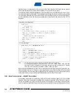
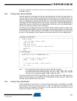
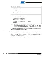
Page 186: ...of samples reduced from 16 to 8 for data sampling and clock recovery and therefore a more accurate baud rate setting and system clock are required when this mode is used For the Transmitter there are...

Page 187: ...d at falling XCK edge If UCPOL is set the data will be changed at falling XCK edge and sampled at rising XCK edge 18 4 Serial Frame A serial frame is defined to be one character of data bits with sync...

Page 188: ...odd parity is used the result of the exclusive or is inverted The relation between the parity bit and data bits is as follows Peven Parity bit using even parity Podd Parity bit using odd parity dn Da...

Page 189: ...interrupts and so on However many applications use a fixed setting of the baud and control registers and for these types of applications the initialization code can be placed directly in the main rou...

Page 190: ...n be used For the assembly code the data to be sent is assumed to be stored in Register R16 Note 1 The example code assumes that the part specific header file is included For I O Registers located in...

Page 191: ...terrupts The Data Register Empty UDRE flag indicates whether the transmit buffer is ready to receive new data This bit is set when the transmit buffer is empty and cleared when the transmit buffer con...

Page 192: ...ansmitter The disabling of the Transmitter setting the TXEN to zero will not become effective until ongo ing and pending transmissions are completed i e when the Transmit Shift Register and Transmit B...

Page 193: ...read from the RXB8 bit in UCSRB before reading the low bits from the UDR This rule applies to the FE DOR and UPE Status Flags as well Read status from UCSRA then data from UDR Reading the UDR I O loc...

Page 194: ...to accept new data as early as possible Assembly Code Example 1 USART_Receive Wait for data to be received sbis UCSRA RXC0 rjmp USART_Receive Get status and 9th bit then data from buffer lds r18 UCSRA...

Page 195: ...lags must be set to zero when the UCSRA is written for upward compatibility of future USART implementations None of the error flags can generate interrupts The Frame Error FE flag indicates the state...

Page 196: ...Parity Error The UPE bit is set if the next character that can be read from the receive buffer had a Parity Error when received and the Parity Checking was enabled at that point UPM1 1 This bit is val...

Page 197: ...illustrates the sampling process of the start bit of an incoming frame The sample rate is 16 times the baud rate for Normal mode and eight times the baud rate for Double Speed mode The hor izontal arr...

Page 198: ...els the received bit is registered to be a logic 1 If two or all three samples have low levels the received bit is registered to be a logic 0 This majority voting process acts as a low pass filter for...

Page 199: ...r majority voting SF 8 for normal speed and SF 4 for Double Speed mode SM Middle sample number used for majority voting SM 9 for normal speed and SM 5 for Double Speed mode Rslow is the ratio of the s...

Page 200: ...ransmitter is unaffected by the MPCM setting but has to be used differently when it is a part of a system utilizing the Multi processor Communication mode 18 9 1 MPCM Protocol If the Receiver is set u...

Page 201: ...frames are used the Transmitter must be set to use two stop bit USBS 1 since the first stop bit is used for indicating the frame type 18 10 USART Register Description 18 10 1 USART I O Data Register U...

Page 202: ...t the Transmitter is ready This bit is available in both USART and EUSART modes Bit 4 FE Frame Error This bit is set if the next character in the receive buffer had a Frame Error when received I e whe...

Page 203: ...Transmit Complete interrupt will be generated only if the TXCIE bit is written to one the Global Interrupt Flag in SREG is writ ten to one and the TXC bit in UCSRA is set This bit is available for bo...

Page 204: ...ing the low bits to UDR When the EUSART mode is enable and configured in 17 bits transmit mode this bit contains the seventeenth bit See EUSART section 18 10 4 USART Control and Status Register C UCSR...

Page 205: ...vior and the EUSB bit of the EUSART allows to configure the number of stop bit for the receiver in this mode Bit 2 1 UCSZ1 0 Character Size The UCSZ1 0 bits combined with the UCSZ2 bit in UCSRB sets t...

Page 206: ...ate prescaler 18 11 Examples of Baud Rate Setting For standard crystal resonator and external oscillator frequencies the most commonly used baud rates for asynchronous operation can be generated by us...

Page 207: ...230 4k 0 0 0 250k 500k 1M Max 1 62 5 kbps 125 kbps 115 2 kbps 230 4 Kbps 125 kpbs 250 kbps 1 UBRR 0 Error 0 0 Table 18 10 Examples of UBRR Settings for Commonly Frequencies Continued Baud Rate bps fcl...

Page 208: ...250 kbps 0 5 Mbps 460 8 kpbs 921 6 kbps 1 UBRR 0 Error 0 0 Table 18 10 Examples of UBRR Settings for Commonly Frequencies Continued Baud Rate bps fclkio 3 6864 MHz fclkio 4 0000 MHz fclkio 7 3728 MHz...

Page 209: ...9600 51 0 2 103 0 2 64 0 2 129 0 2 71 0 0 143 0 0 14 4k 34 0 8 68 0 6 42 0 9 86 0 2 47 0 0 95 0 0 19 2k 25 0 2 51 0 2 32 1 4 64 0 2 35 0 0 71 0 0 28 8k 16 2 1 34 0 8 21 1 4 42 0 9 23 0 0 47 0 0 38 4k...

Page 210: ...essible The EUSART supports more serial frame formats than the standard USART interface Table 18 12 Examples of UBRR Settings for Commonly Frequencies Continued Baud Rate bps fclkio 12 0000 MHz fclkio...

Page 211: ...t bit 5 6 7 8 9 13 14 15 16 17 data bits data bits and start bit level encoded or Manchester encoded data transmition MSB or LSB first bit ordering no even or odd parity bit 1 or 2 stop bits Stop bits...

Page 212: ...f odd parity is used the result of the exclusive or is inverted The relation between the parity bit and data bits is as follows Peven Parity bit using even parity Podd Parity bit using odd parity dn D...

Page 213: ...arity of the stop bits is not configurable the interface allows to read the 2 stops bits value by software The Manchester decoder is enable when the EUSART is configured in Manchester mode and the RXE...

Page 214: ...2X on page 187 This mode of operation is not allowed in manchester bit coding Each bit time in the Manchester serial frame is divided into two phases See Figure 19 4 The counter counts during the firs...

Page 215: ...error FE of the USCRA register is not used the EUSART generates a dedicated Frame Error Manchester FEM when a data data bit is not detected during the detection window See Figure 19 5 N2 N1 N3 Manche...

Page 216: ...tart bit detection phase Thus when a Manchester framing error is detected within a frame the receiver will process the rest of the frame as a new incomming frame and generate other FEM errors Internal...

Page 217: ...USART section 19 4 3 Sending Frames with 9 13 14 15 or 16 Data Bit In these configurations the most significant bits 9 13 14 15 or 16 should be loaded in the EUDR register before the low byte of the...

Page 218: ...contain data to be transmitted 19 4 7 Data Reception EUSART Receiver 19 5 Data Reception EUSART Receiver The EUSART Receiver is enabled by writing the Receive Enable RXEN bit in the UCSRB Reg ister t...

Page 219: ...The EUSART Receiver has the same USART flag that indicates the Receiver state See Receive Complete Flag and Interrupt in USART section 19 5 5 Receiver Error Flags When the EUSART is not configured in...

Page 220: ...ister See description for UDR register in USART 19 6 2 EUSART I O Data Register EUDR Bit 7 0 RxB15 8 Receive Data Buffer read access Bit 7 0 TxB15 8 Transmit Data Buffer write access This register pro...

Page 221: ...to zero by the Receiver In transmitter mode the data should be written MSB first The data transmission starts when the UDR register is written In these modes the RxB8 TxB8 registers are not used Figur...

Page 222: ...CSRA Read Write R W R W R W R W R W R W R W R W Initial Value 0 0 1 1 0 0 1 1 Table 19 1 UTxS Bits Settings UTxS3 UTxS2 UTxS1 UTxS0 Transmit Character Size 0 0 0 0 5 bit 0 0 0 1 6 bit 0 0 1 0 7 bit 0...

Page 223: ...tter in EUSART mode is configurable throught the USBS bit of in the of the USART Bit 2 Reserved Bit This bit is reserved for future use For compatibilty with future devices this bit must be written to...

Page 224: ...the receive buffer UDR is read Bit 2 F1617 When the receiver is configured for 16 or 17 bits in Manchester encoded mode this bit indicates if the received frame is 16 or 17 bits lenght Cleared indicat...

Page 225: ...pted if the baud rate is changed MUBRR H L FCLKIO baud rate frequency Bit 15 14 13 12 11 10 9 8 MUBRR 15 8 MUBRRH MUBRR 7 0 MUBRRL 7 6 5 4 3 2 1 0 Read Write R W R W R W R W R W R W R W R W R W R W R...

Page 226: ...r than the voltage selected by the ACnM multiplexer on the negative input the Analog Comparator output ACnO is set The comparator is a clocked comparator A new comparison is done on the falling edge o...

Page 227: ...parator 0 Bit 6 AC0IE Analog Comparator 0 Interrupt Enable bit Set this bit to enable the analog comparator 0 interrupt Clear this bit to disable the analog comparator 0 interrupt Bit 5 4 AC0IS1 AC0IS...

Page 228: ...his bit to enable the analog comparator 1 interrupt Clear this bit to disable the analog comparator 1 interrupt Bit 5 4 AC1IS1 AC1IS0 Analog Comparator 1 Interrupt Select bit Table 20 1 Interrupt sens...

Page 229: ...to disable this function In this case no connection between the Analog Compara tor and the input capture function exists Bit 2 1 0 AC1M2 AC1M1 AC1M0 Analog Comparator 1 Multiplexer register These 3 b...

Page 230: ...the clock of the microcontroller and the clock of the analog comparators Clear this bit to have the same clock frequency for the microcontroller and the analog comparators Bit 6 AC2IF Analog Comparato...

Page 231: ...Bit 1 AC1O Analog Comparator 1 Output Bit AC1O bit is directly the output of the Analog comparator 1 Set when the output of the comparator is high Cleared when the output comparator is low Bit 0 AC0O...

Page 232: ...01 08 AT90PWM2 3 2B 3B analog signal is applied to one of these pins and the digital input from this pin is not needed this bit should be written logic one to reduce power consumption in the digital...

Page 233: ...which allows eleven single ended input The single ended voltage inputs refer to 0V GND The device also supports 2 differential voltage input combinations which are equipped with a programmable gain s...

Page 234: ...C ADATE ADIF ADMUX ADCSRA ADTS2 ADTS1 ADTS0 ADASCR ADCSRB Edge Detector Sources ADC0 ADC1 ADC2 ADC3 ADC4 ADC5 ADC6 ADC7 AMP1 ADC8 AMP1 ADC9 ADC10 AMP0 AMP0 AMP0CSR AMP1CSR SAR 10 10 ADCH ADCL Coarse F...

Page 235: ...mpleted before ADCH is read neither register is updated and the result from the conversion is lost When ADCH is read ADC access to the ADCH and ADCL Registers is re enabled The ADC has its own interru...

Page 236: ...conversion independently of how the conversion was started 21 4 Prescaling and Conversion Timing Figure 21 3 ADC Prescaler By default the successive approximation circuitry requires an input clock fr...

Page 237: ...hen Auto Triggering is used the prescaler is reset when the trigger event occurs This assures a fixed delay from the trigger event to the start of conversion In this mode the sample and hold takes pla...

Page 238: ...re the conversion completes ADIF in ADCSRA is set Note that the conversion starts on the following rising ADC clock edge after ADSC is written The user is thus advised not to write new channel or refe...

Page 239: ...changed one ADC clock cycle after writing one to ADSC However the simplest method is to wait for the first conversion to complete and then change the channel selection Since the next conversion has al...

Page 240: ...uch sleep modes to avoid excessive power consumption If the ADC is enabled in such sleep modes and the user wants to perform differential conver sions the user is advised to switch the ADC off and on...

Page 241: ...2 The AVCC pin on the device should be connected to the digital VCC supply voltage via an LC network as shown in Figure 21 9 3 Use the ADC noise canceler function to reduce induced noise from the CPU...

Page 242: ...ults Using this kind of software based offset correction offset on any channel can be reduced below one LSB 21 6 4 ADC Accuracy Definitions An n bit single ended ADC converts a voltage linearly betwee...

Page 243: ...ared to an ideal transition for any code Ideal value 0 LSB Figure 21 12 Integral Non linearity INL Differential Non linearity DNL The maximum deviation of the actual code width the interval between tw...

Page 244: ...reference see Table 21 3 on page 247 and Table 21 4 on page 248 0x000 represents analog ground and 0x3FF represents the selected reference voltage If differential channels are used the result is where...

Page 245: ...60 400 0x270 Table 21 2 Correlation Between Input Voltage and Output Codes VADCn Read code Corresponding decimal value VADCm VREF GAIN 0x1FF 511 VADCm 0 999 VREF GAIN 0x1FF 511 VADCm 0 998 VREF GAIN 0...

Page 246: ...oltage reference for the ADC The different setting are shown in Table 21 3 If these bits are changed during a conversion the change will not take effect until this conversion is complete it means whil...

Page 247: ...et this bit to start a conversion in single conversion mode or to start the first conversion in free running mode Cleared by hardware when the conversion is complete Writing this bit to zero has no ef...

Page 248: ...7 ADHSM ADC High Speed Mode Writing this bit to one enables the ADC High Speed mode Set this bit if you wish to convert with an ADC clock frequency higher than 200KHz Bit 4 ADASCR Analog to Digital Co...

Page 249: ...Analog Comparator 0 0 0 1 0 External Interrupt Request 0 0 0 1 1 Timer Counter0 Compare Match 0 1 0 0 Timer Counter0 Overflow 0 1 0 1 Timer Counter1 Compare Match B 0 1 1 0 Timer Counter1 Overflow 0 1...

Page 250: ...e Register 0 DIDR0 Bit 7 0 ADC7D ADC0D ACMP2 1 and ADC7 0 Digital Input Disable 1 0 1 0 PSC2ASY Event 1 1 0 1 1 Reserved 1 1 0 0 Reserved 1 1 0 1 Reserved 1 1 1 0 Reserved 1 1 1 1 Reserved 1 For trigg...

Page 251: ...PSC events See Synchronization Source Description in One Two Four Ramp Modes on page 162 and Synchronization Source Descrip tion in Centered Mode on page 163 or to the internal clock CKADC equal to e...

Page 252: ...not possible unless the ADSC bit in ADCSRA is set by soft after each conversion Only PSC sources can auto trigger the amplified conversion In this case the core must have a clock synchronous with the...

Page 253: ...recaution to take is to be sure that the trig signal PSC frequency is lower than ADCclk 4 Figure 21 16 Amplifier synchronization timing diagram for AT90PWM2B 3B With change on analog input signal Figu...

Page 254: ...AT90PWM2 3 2B 3B Valid sample Signal to be measu red AMPLI_clk Sync Clock CK ADC PS Cn_ASY PSC Block ADSC ADC Activity ADC ADC Sampling ADC Conv ADC Sampling ADC Conv ADC Sampling Aborted ADCResult Re...

Page 255: ...d on ADCH and ADCL register which contain respectively the most significant bits and the less significant bits 21 10 1 Amplifier 0 Control and Status register AMP0CSR AMP0TS1AMP0TS0 AMP0EN AMP0IS AMP0...

Page 256: ...Trigger Source Selection Bits In accordance with the Table 21 9 these 2 bits select the event which will generate the trigger for the amplifier 0 This trigger source is necessary to start the conversi...

Page 257: ...during at least 4 Amplifier synchronization clock periods Bit 1 0 AMP1TS1 AMP1TS0 Amplifier 1 Trigger Source Selection Bits In accordance with the Table 21 11 these 2 bits select the event which will...

Page 258: ...to drive worst case a 1nF capacitance in parallel with a resistor higher than 33K load with a time constant around 1us Response time and power consumption are improved by reducing the load reducing th...

Page 259: ...ng the DAC Auto Trigger Enable bit DAATE in DACON The trigger source is selected by setting the DAC Trigger Select bits DATS in DACON See description of the DATS bits for a list of the trigger sources...

Page 260: ...AVCC and 2 56V as reference selection The first DAC conversion result after switching reference voltage source may be inaccurate and the user is advised to discard this result 22 4 DAC Register Descri...

Page 261: ...il DACH has not been written too So the normal way to write a 10 bit value in the DAC register is firstly to write DACL the DACH In order to work easily with only 8 bits there is the possibility to le...

Page 262: ...e update can only be done after having written respectively DACL and DACH registers It is possible to work on 8 bit configuration by only writ ing the DACH value In this case update is done each trigg...

Page 263: ...l the program flow execute AVR instructions in the CPU and to program the different non volatile memories 23 3 Physical Interface When the debugWIRE Enable DWEN Fuse is programmed and Lock bits are un...

Page 264: ...the debugWIRE is enabled The debugWIRE system accurately emulates all I O functions when running at full speed i e when the program in the CPU is running When the CPU is stopped care must be taken wh...

Page 265: ...section is the section of the Flash that is used for storing the application code The protection level for the Application section can be selected by the application Boot Lock bits Boot Lock bits 0 s...

Page 266: ...e interrupts should either be disabled or moved to the Boot Loader sec tion The Boot Loader section is always located in the NRWW section The RWW Section Busy bit RWWSB in the Store Program Memory Con...

Page 267: ...ile Write vs No Read While Write Read While Write RWW Section No Read While Write NRWW Section Z pointer Addresses RWW Section Z pointer Addresses NRWW Section CPU is Halted During the Operation Code...

Page 268: ...e general Write Lock Lock Bit mode 2 does not control the programming of the Flash memory by SPM instruction Similarly the general Read Write Lock Lock Bit mode 1 does not control reading nor writing...

Page 269: ...to the Application section and LPM executing from the Boot Loader section is not allowed to read from the Application section If Interrupt Vectors are placed in the Boot Loader section interrupts are...

Page 270: ...y with a Page Erase or a Page Write SPMEN is set If the RWWSRE bit is writ ten while the Flash is being loaded the Flash load operation will abort and the data loaded will be lost Bit 3 BLBSET Boot Lo...

Page 271: ...ts will have no effect 24 6 Addressing the Flash During Self Programming The Z pointer is used to address the SPM commands Since the Flash is organized in pages see Table 25 11 on page 285 the Program...

Page 272: ...e If only a part of the page needs to be changed the rest of the page must be stored for example in the temporary page buffer before the erase and then be rewritten When using alternative 1 the Boot L...

Page 273: ...W section can be read during the Page Write Page Write to the NRWW section The CPU is halted during the operation 24 7 4 Using the SPM Interrupt If the SPM interrupt is enabled the SPM interrupt will...

Page 274: ...the BLBSET and SPMEN bits in SPMCSR When an LPM instruc tion is executed within three CPU cycles after the BLBSET and SPMEN bits are set in SPMCSR the value of the Lock bits will be loaded in the dest...

Page 275: ...if the operating volt age matches the detection level If not an external low VCC reset protection circuit can be used If a reset occurs while a write operation is in progress the write operation will...

Page 276: ...looplo 2 use subi for PAGESIZEB 256 brne Wrloop execute Page Write subi ZL low PAGESIZEB restore pointer sbci ZH high PAGESIZEB not required for PAGESIZEB 256 ldi spmcrval 1 PGWRT 1 SPMEN call Do_spm...

Page 277: ...the parameters used in the description of the self program ming are given Note The different BOOTSZ Fuse configurations are shown in Figure 24 2 Table 24 6 Boot Size Configuration BOOTSZ1 BOOTSZ0 Boo...

Page 278: ...nding Z value 1 Description PCMSB 11 Most significant bit in the Program Counter The Program Counter is 12 bits PC 11 0 PAGEMSB 4 Most significant bit which is used to address the words within one pag...

Page 279: ...to the Application section 3 0 0 SPM is not allowed to write to the Application section and LPM executing from the Boot Loader section is not allowed to read from the Application section If Interrupt...

Page 280: ...0 PSCOUT01 are forced at reset to low level or high level according to PSCRV fuse bit In this second case PSCOUT00 PSCOUT01 keep the forced state until PSOC0 register is written If PSC1RB fuse equals...

Page 281: ...es will have no effect until the part leaves Programming mode This does not apply to the EESAVE Fuse which will take effect once it is programmed The fuses are also latched on Power up in Normal mode...

Page 282: ...e resides in the high byte of address 0x000 in the signature address space During reset this byte is automatically written into the OSCCAL Register to ensure correct frequency of the calibrated RC Osc...

Page 283: ...byte 1 selects High byte XA0 PD5 I XTAL Action Bit 0 XA1 PD6 I XTAL Action Bit 1 PAGEL PD7 I Program memory and EEPROM Data Page Load BS2 PE2 I Byte Select 2 0 selects Low byte 1 selects 2 nd High by...

Page 284: ...0001 0001 Write EEPROM 0000 1000 Read Signature Bytes and Calibration byte 0000 0100 Read Fuse and Lock bits 0000 0010 Read Flash 0000 0011 Read EEPROM Table 25 11 No of Words in a Page and No of Page...

Page 285: ...tually reaches 4 5 5 5V before giving any parallel programming commands 6 Exit Programming mode by power the device down or by bringing RESET pin to 0V 25 8 2 Considerations for Efficient Programming...

Page 286: ...00 0xFF 3 Give XTAL1 a positive pulse This loads the data byte D Load Data High Byte 1 Set BS1 to 1 This selects high data byte 2 Set XA1 XA0 to 01 This enables data loading 3 Set DATA Data high byte...

Page 287: ...lse This loads the command and the internal write signals are reset Figure 25 2 Addressing the Flash Which is Organized in Pages 1 Note 1 PCPAGE and PCWORD are listed in Table 25 11 on page 285 Figure...

Page 288: ...r is filled L Program EEPROM page 1 Set BS1 to 0 2 Give WR a negative pulse This starts programming of the EEPROM page RDY BSY goes low 3 Wait until to RDY BSY goes high before programming the next pa...

Page 289: ...BSY to go high 25 8 9 Programming the Fuse High Bits The algorithm for programming the Fuse High bits is as follows refer to Programming the Flash on page 287 for details on Command and Data loading 1...

Page 290: ...and Lock Bits The algorithm for reading the Fuse and Lock bits is as follows refer to Programming the Flash on page 287 for details on Command loading 1 A Load Command 0000 0100 2 Set OE to 0 BS2 to...

Page 291: ...ing the Calibration Byte The algorithm for reading the Calibration byte is as follows refer to Programming the Flash on page 287 for details on Command and Address loading 1 A Load Command 0000 1000 2...

Page 292: ...bol Parameter Min Typ Max Units VPP Programming Enable Voltage 11 5 12 5 V IPP Programming Enable Current 250 A tDVXH Data and Control Valid before XTAL1 High 67 ns tXLXH XTAL1 Low to XTAL1 High 200 n...

Page 293: ...mming is listed Not all parts use the SPI pins dedicated for the internal SPI interface tXLPH XTAL1 Low to PAGEL high 0 ns tPLXH PAGEL low to XTAL1 high 150 ns tBVPH BS1 Valid before PAGEL High 67 ns...

Page 294: ...g edge of SCK See Figure 25 11 for timing details To program and verify the AT90PWM2 2B 3 3B in the serial programming mode the following sequence is recommended See four byte instruction formats in T...

Page 295: ...l give the value 0xFF At the time the device is ready for a new page the programmed value will read correctly This is used to determine when the next page can be writ ten Note that the entire page is...

Page 296: ...00a aaaa bbxx xxxx xxxx xxxx Write Program Memory Page at address a b Read EEPROM Memory 1010 0000 000x xxaa bbbb bbbb oooo oooo Read data o from EEPROM memory at address a b Write EEPROM Memory 1100...

Page 297: ...00 0000 xxxx xxxx oooo oooo Read Fuse bits 0 programmed 1 unprogrammed See Table XXX on page XXX for details Read Fuse High bits 0101 1000 0000 1000 xxxx xxxx oooo oooo Read Fuse High bits 0 pro gramm...

Page 298: ...manent dam age to the device This is a stress rating only and functional operation of the device at these or other conditions beyond those indicated in the operational sections of this specification i...

Page 299: ...9VCC 2 VCC 0 5 V VIL3 Input Low Voltage RESET pin as I O 0 5 0 2VCC 1 V VIH3 Input High Voltage RESET pin as I O 0 8VCC 2 VCC 0 5 V VOL Output Low Voltage 3 Port B C D and XTAL1 XTAL2 pins as I O IOL...

Page 300: ...e sum of all IOH for all ports should not exceed 400 mA 2 The sum of all IOH for ports B6 B7 C0 C1 D0 D3 E0 should not exceed 150 mA 3 The sum of all IOH for ports B0 B1 C2 C3 D4 E1 E2 should not exce...

Page 301: ...ternal Clock Drive Table 26 1 Calibration Accuracy of Internal RC Oscillator Frequency VCC Temperature Calibration Accuracy Factory Calibration 8 0 MHz 3V 25 C 10 User Calibration 7 3 8 1 MHz 2 7V 5 5...

Page 302: ...m Frequency vs VCC AT90PWM2 2B 3 3B 26 5 PLL Characteristics Note While connected to external clock or external oscillator PLL Input Frequency must be selected to provide outputs with frequency in acc...

Page 303: ...od Master See Table 64 ns 2 SCK high low Master 50 duty cycle 3 Rise Fall time Master 3 6 4 Setup Master 10 5 Hold Master 10 6 Out to SCK Master 0 5 tsck 7 SCK to out Master 10 8 SCK to out high Maste...

Page 304: ...305 4317I AVR 01 08 AT90PWM2 3 2B 3B Figure 26 4 SPI Interface Timing Requirements Slave Mode MISO Data Output SCK CPOL 1 MOSI Data Input SCK CPOL 0 SS MSB LSB LSB MSB 10 11 11 12 13 14 17 15 9 X 16...

Page 305: ...ADC clock 500 kHz 2 3 LSB Differential Conversion VREF 2 56V ADC clock 1MHz 3 1 4 LSB Integral Non linearity Single Ended Conversion VCC 4 5V VREF 2 56V ADC clock 1MHz 1 1 1 5 LSB Single Ended Conver...

Page 306: ...ion 8 320 s Clock Frequency 50 2000 kHz AVCC Analog Supply Voltage VCC 0 3 VCC 0 3 V VREF Reference Voltage Single Ended Conversion 2 0 AVCC V Differential Conversion 2 0 AVCC 0 2 V VIN Input voltage...

Page 307: ...1 Note 1 The timing requirements shown in Figure 26 5 i e tDVXH tXHXL and tXLDX also apply to load ing operation Data Contol DATA XA0 1 BS1 BS2 XTAL1 tXHXL tWLWH tDVXH tXLDX tPLWL tWLRH WR RDY BSY PAG...

Page 308: ...VPP Programming Enable Voltage 11 5 12 5 V IPP Programming Enable Current 250 A tDVXH Data and Control Valid before XTAL1 High 67 ns tXLXH XTAL1 Low to XTAL1 High 200 ns tXHXL XTAL1 Pulse Width High...

Page 309: ...gister on page 37 for details The power consumption in Power down mode is independent of clock selection The current consumption is a function of several factors such as operating voltage operating fr...

Page 310: ...pply Current vs Frequency 1 24 MHz ACTIVE SUPPLY CURRENT vs LOW FREQUENCY 5 5 V 5 0 V 4 5 V 4 0 V 3 3 V 3 0 V 2 7 V 0 0 2 0 4 0 6 0 8 1 1 2 1 4 1 6 0 0 1 0 2 0 3 0 4 0 5 0 6 0 7 0 8 0 9 1 Frequency MH...

Page 311: ...y Current vs VCC Internal PLL Oscillator 16 MHz ACTIVE SUPPLY CURRENT vs VCC INTERNAL RC OSCILLATOR 8 MHz 105 C 85 C 25 C 40 C 0 1 2 3 4 5 6 7 8 9 2 2 5 3 3 5 4 4 5 5 5 5 VCC V I CC mA ACTIVE SUPPLY C...

Page 312: ...Frequency 1 24 MHz IDLE SUPPLY CURRENT vs LOW FREQUENCY 5 5 V 5 0 V 4 5 V 4 0 V 3 3 V 3 0 V 2 7 V 0 0 05 0 1 0 15 0 2 0 25 0 3 0 35 0 4 0 45 0 0 1 0 2 0 3 0 4 0 5 0 6 0 7 0 8 0 9 1 Frequency MHz I CC...

Page 313: ...below can be used to calculate the additional current consumption for the different I O modules in Active and Idle mode The enabling or disabling of the I O modules IDLE SUPPLY CURRENT vs VCC INTERNAL...

Page 314: ...1 but in active mode instead From Table 27 2 second column we see that we need to add 3 3 for the USART 4 8 for the SPI and 2 0 for the TIMER1 module Reading from Figure 27 1 we find that the active c...

Page 315: ...consumption without the I O modules to be 7 0mA from Figure 27 2 Then by using the numbers from Table 27 2 second column we find the total current consumption 27 3 Power Down Supply Current Figure 27...

Page 316: ...Pull Up Resistor Current vs Input Voltage VCC 5V POWER DOWN SUPPLY CURRENT vs VCC WATCHDOG TIMER ENABLED 105 C 85 C 25 C 40 C 0 2 4 6 8 10 12 14 2 2 5 3 3 5 4 4 5 5 5 5 VCC V I CC uA I O PIN includin...

Page 317: ...tor Current vs Reset Pin Voltage VCC 5V I O PIN including PE1 PE2 PULL UP RESISTOR CURRENT vs INPUT VOLTAGE Vcc 2 7 V 105 C 85 C 25 C 40 C 10 0 10 20 30 40 50 60 70 80 90 0 0 5 1 1 5 2 2 5 3 VOP V I O...

Page 318: ...27 15 I O Pin Source Current vs Output Voltage VCC 5V PE0 and RESET PULL UP RESISTOR CURRENT vs INPUT VOLTAGE Vcc 2 7 V 105 C 85 C 25 C 40 C 0 10 20 30 40 50 60 70 0 0 5 1 1 5 2 2 5 3 VOP V I OP uA I...

Page 319: ...n Sink Current vs Output Voltage VCC 5V I O PIN including PE1 PE2 SOURCE CURRENT vs OUTPUT VOLTAGE Vcc 2 7 V 105 C 85 C 25 C 40 C 0 5 10 15 20 25 0 0 5 1 1 5 2 2 5 3 VOH V I OH mA I O PIN including PE...

Page 320: ...Input Threshold Voltage vs VCC VIH I O Pin Read As 1 I O PIN including PE1 PE2 SINK CURRENT vs OUTPUT VOLTAGE Vcc 2 7 V 105 C 85 C 25 C 40 C 5 0 5 10 15 20 25 0 0 5 1 1 5 2 2 5 3 VOL V I OL mA I O PI...

Page 321: ...I O Pin Input HysteresisVoltage vs VCC I O PIN including PE1 PE2 INPUT THRESHOLD VOLTAGE vs VCC VIL IO PIN READ AS 0 105 C 85 C 25 C 40 C 0 0 5 1 1 5 2 2 5 2 2 5 3 3 5 4 4 5 5 5 5 VCC V Threshold V I...

Page 322: ...t Threshold Voltage vs VCC VIL Reset Pin Read As 0 RESET INPUT THRESHOLD VOLTAGE vs VCC VIH RESET PIN READ AS 1 105 C 85 C 25 C 40 C 0 0 5 1 1 5 2 2 5 2 2 5 3 3 5 4 4 5 5 5 5 VCC V Threshold V RESET I...

Page 323: ...old Voltage vs VCC XTAL1 Pin Read As 1 RESET PIN INPUT HYSTERESIS vs VCC 105 C 85 C 25 C 40 C 0 0 1 0 2 0 3 0 4 0 5 0 6 2 2 5 3 3 5 4 4 5 5 5 5 VCC V Input Hysteresis V XTAL1 INPUT THRESHOLD VOLTAGE v...

Page 324: ...reshold Voltage vs VCC PE0 Pin Read As 1 XTAL1 INPUT THRESHOLD VOLTAGE vs VCC XTAL1 PIN READ AS 0 105 C 85 C 25 C 40 C 0 0 5 1 1 5 2 2 5 3 3 5 4 2 2 5 3 3 5 4 4 5 5 5 5 VCC V Threshold V PE0 INPUT THR...

Page 325: ...Thresholds vs Temperature BODLEVEL Is 4 3V PE0 INPUT THRESHOLD VOLTAGE vs VCC VIL PE0 PIN READ AS 0 105 C 85 C 25 C 40 C 0 0 5 1 1 5 2 2 5 2 2 5 3 3 5 4 4 5 5 5 5 VCC V Threshold V BOD THRESHOLDS vs T...

Page 326: ...B to allow almost full scale use BOD THRESHOLDS vs TEMPERATURE BODLV IS 2 7 V Rising Vcc Falling Vcc 2 68 2 7 2 72 2 74 2 76 2 78 2 8 2 82 50 40 30 20 10 0 10 20 30 40 50 60 70 80 90 100 110 120 Tempe...

Page 327: ...e 27 8 Analog Reference Figure 27 33 AREF Voltage vs VCC ANALOG COMPARATOR TYPICAL OFFSET VOLTAGE vs COMMON MODE VOLTAGE Vcc 3 0 V 0 0 005 0 01 0 015 0 02 0 025 0 03 0 035 0 04 0 045 0 0 5 1 1 5 2 2 5...

Page 328: ...al Oscillator Speed Figure 27 35 Watchdog Oscillator Frequency vs VCC AREF VOLTAGE vs TEMPERATURE 5 5 5 4 5 3 2 52 2 53 2 54 2 55 2 56 2 57 2 58 2 59 60 40 20 0 20 40 60 80 100 120 Temperature Aref V...

Page 329: ...8MHz RC OSCILLATOR FREQUENCY vs TEMPERATURE 10000 Cycles sampled w ith 250nS 7 4 7 5 7 6 7 7 7 8 7 9 8 8 1 8 2 8 3 8 4 50 40 30 20 10 0 10 20 30 40 50 60 70 80 90 100 110 Temperature OSCCAL MHz 2 7 5...

Page 330: ...7 10 Current Consumption of Peripheral Units Figure 27 39 Brownout Detector Current vs VCC 0 2 4 6 8 10 12 14 16 18 0 16 32 48 64 80 96 112 128 144 160 176 192 208 224 240 OSCCAL F RC MHz BROWNOUT DET...

Page 331: ...1 Aref Current vs VCC ADC at 1 MHz AREF vs VCC ADC AT 50 KHz 85 C 25 C 40 C 150 200 250 300 350 400 450 500 1 5 2 2 5 3 3 5 4 4 5 5 5 5 VCC V I CC uA TEMPLATE TO BE CHARACTERIZED AREF vs VCC ADC AT 1...

Page 332: ...ent vs VCC Figure 27 43 Programming Current vs VCC ANALOG COMPARATOR CURRENT vs VCC 105 C 85 C 25 C 40 C 0 10 20 30 40 50 60 70 80 2 2 5 3 3 5 4 4 5 5 5 5 VCC V I CC uA PROGRAMMING CURRENT vs V 85 C 2...

Page 333: ...Excluding Current through the Reset Pull up RESET SUPPLY CURRENT vs VCC EXCLUDING CURRENT THROUGH THERESET PULLUP 5 5 V 5 0 V 4 5 V 4 0 V 3 3 V 3 0 V 2 7 V 0 0 02 0 04 0 06 0 08 0 1 0 12 0 14 0 16 0 1...

Page 334: ...gure 27 47 Reset Pulse Width vs VCC RESET CURRENT vs VCC CLOCK STOPPED EXCLUDING CURRENT THROUGH THE RESET PULLUP 105 C 85 C 25 C 40 C 0 01 0 0 01 0 02 0 03 0 04 0 05 2 2 5 3 3 5 4 4 5 5 5 5 VCC V I C...

Page 335: ...E2 OCR1SAL page 163 0xE1 Reserved 0xE0 PSOC1 PSYNC11 PSYNC10 POEN1B POEN1A page 162 0xDF PICR0H page 170 0xDE PICR0L page 170 0xDD PFRC0B PCAE0B PISEL0B PELEV0B PFLTE0B PRFM0B3 PRFM0B2 PRFM0B1 PRFM0B0...

Page 336: ...Reserved 0x9B Reserved 0x9A Reserved 0x99 Reserved 0x98 Reserved 0x97 Reserved 0x96 Reserved 0x95 Reserved 0x94 Reserved 0x93 Reserved 0x92 Reserved 0x91 Reserved 0x90 Reserved 0x8F Reserved 0x8E Rese...

Page 337: ...ERS SPMEN page 271 0x36 0x56 Reserved 0x35 0x55 MCUCR SPIPS PUD IVSEL IVCE page 60 page 69 0x34 0x54 MCUSR WDRF BORF EXTRF PORF page 50 0x33 0x53 SMCR SM2 SM1 SM0 SE page 41 0x32 0x52 MSMCR Monitor St...

Page 338: ...TD and LD LDS LDD instructions can be used 0x1A 0x3A GPIOR2 GPIOR27 GPIOR26 GPIOR25 GPIOR24 GPIOR23 GPIOR22 GPIOR21 GPIOR20 page 27 0x19 0x39 GPIOR1 GPIOR17 GPIOR16 GPIOR15 GPIOR14 GPIOR13 GPIOR12 GPI...

Page 339: ...k Relative Subroutine Call PC PC k 1 None 3 ICALL Indirect Call to Z PC Z None 3 RET Subroutine Return PC STACK None 4 RETI Interrupt Return PC STACK I 4 CPSE Rd Rr Compare Skip if Equal if Rd Rr PC...

Page 340: ...d K None 1 LD Rd X Load Indirect Rd X None 2 LD Rd X Load Indirect and Post Inc Rd X X X 1 None 2 LD Rd X Load Indirect and Pre Dec X X 1 Rd X None 2 LD Rd Y Load Indirect Rd Y None 2 LD Rd Y Load Ind...

Page 341: ...NOP No Operation None 1 SLEEP Sleep see specific descr for Sleep function None 1 WDR Watchdog Reset see specific descr for WDR timer None 1 BREAK Break For On chip Debug Only None N A Mnemonics Operan...

Page 342: ...ot recommended for new designs use PWM2B for your developments Note PWM3 is not recommended for new designs use PWM3B for your developments Speed MHz Power Supply Ordering Code Package Operation Range...

Page 343: ...345 4317I AVR 01 08 AT90PWM2 3 2B 3B 31 Package Information Package Type SO24 24 Lead Small Outline Package SO32 32 Lead Small Outline Package QFN32 32 Lead Quad Flat No lead...

Page 344: ...346 4317I AVR 01 08 AT90PWM2 3 2B 3B 31 1 SO24...

Page 345: ...347 4317I AVR 01 08 AT90PWM2 3 2B 3B 31 2 SO32...

Page 346: ...348 4317I AVR 01 08 AT90PWM2 3 2B 3B 31 3 QFN32...

Page 347: ...349 4317I AVR 01 08 AT90PWM2 3 2B 3B...

Page 348: ...programming mode to load a new program version 2 PSC Prescaler The use of PSC s prescaler have the following effects It blocks the sample of PSC inputs until the two first cycles following the set of...

Page 349: ...er Update Registers DACL DACH are not written when the DAC is not enabled Workaround Enable DAC with DAEN before writing in DACL DACH To prevent an unwanted zero out put on DAC pin enable DAC output w...

Page 350: ...uts in mode 14 See PSC Input Mode 14 Fixed Frequency Edge Retrigger PSC and Disactivate Output on page 156 Work around Do not use this mode to desactivate output if retrigger event do not occurs durin...

Page 351: ...mode If the cpu writes in DACH register at the same instant that the selected trigger source occurs and DAC Auto Trigger is enabled the DACH register is not updated by the new value Work around When u...

Page 352: ...on page 160 3 Updated Output Compare SA Register OCRnSAH and OCRnSAL on page 163 4 Updated Output Compare RA Register OCRnRAH and OCRnRAL on page 163 5 Updated Output Compare SB Register OCRnSBH and...

Page 353: ...pdated AMP0 Auto Trigger Source Selection on page 257 10 Updated Amplifier 1Control and Status register AMP1CSR on page 257 11 Updated AMP1 Auto Trigger source selection on page 258 12 Updated DAC Fea...

Page 354: ...Purpose Register File 14 5 6 Stack Pointer 15 5 7 Instruction Execution Timing 15 5 8 Reset and Interrupt Handling 16 6 Memories 19 6 1 In System Reprogrammable Flash Program Memory 19 6 2 SRAM Data...

Page 355: ...T90PWM2 2B 3 3B 57 11 I O Ports 62 11 1 Introduction 62 11 2 Ports as General Digital I O 63 11 3 Alternate Port Functions 67 11 4 Register Description for I O Ports 78 12 External Interrupts 81 13 Ti...

Page 356: ...nput Mode 2 Stop signal Execute Opposite Dead Time and Wait 150 16 11 PSC Input Mode 3 Stop signal Execute Opposite while Fault active 151 16 12 PSC Input Mode 4 Deactivate outputs without changing ti...

Page 357: ...T Register Description 202 18 11 Examples of Baud Rate Setting 207 19 EUSART Extended USART 212 19 1 Features 212 19 2 Overview 212 19 3 Serial Frames 213 19 4 Configuring the EUSART 218 19 5 Data Rec...

Page 358: ...oot Loader Features 266 24 2 Application and Boot Loader Flash Sections 266 24 3 Read While Write and No Read While Write Flash Sections 266 24 4 Boot Loader Lock Bits 269 24 5 Entering the Boot Loade...

Page 359: ...in Driver Strength 320 27 7 Pin Thresholds and Hysteresis 322 27 8 BOD Thresholds and Analog Comparator Offset 327 27 9 Analog Reference 329 27 10 Internal Oscillator Speed 330 27 11 Current Consumpti...

Page 360: ...VR 01 08 AT90PWM2 3 2B 3B 33 4 Changes from 4317D to 4317E 354 33 5 Changes from 4317E to 4317F 354 33 6 Changes from 4317F to 4317G 354 33 7 Changes from 4317G to 4317H 354 33 8 Changes from 4317H to...

Page 361: ...MPLIED OR STATUTORY WARRANTY RELATING TO ITS PRODUCTS INCLUDING BUT NOT LIMITED TO THE IMPLIED WARRANTY OF MERCHANTABILITY FITNESS FOR A PARTICULAR PURPOSE OR NON INFRINGEMENT IN NO EVENT SHALL ATMEL...

Reviews: