69
4317I–AVR–01/08
AT90PWM2/3/2B/3B
When this bit is written to one, the pull-ups in the I/O ports are disabled even if the DDxn and
PORTxn Registers are configured to enable the pull-ups ({DDxn, PORTxn} = 0b01). Se
11.3.2
Alternate Functions of Port B
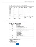
The Port B pins with alternate functions are shown in
.
The alternate pin configuration is as follows:
• PSCOUT01/ADC4/SCK – Bit 7
PSCOUT01: Output 1 of PSC 0.
ADC4, Analog to Digital Converter, input channel 4
.
SCK: Master Clock output, Slave Clock input pin for SPI channel. When the SPI is enabled as a
slave, this pin is configured as an input regardless of the setting of DDB7. When the SPI is
enabled as a master, the data direction of this pin is controlled by DDB7. When the pin is forced
to be an input, the pull-up can still be controlled by the PORTB7 bit.
• ADC7/ICP1B/PSCOUT11 – Bit 6
ADC7, Analog to Digital Converter, input channel 7
.
ICP1B, Input Capture Pin: The PB6 pin can act as an Input Capture Pin for Timer/Counter1.
PSCOUT11: Output 1 of PSC 1.
• ADC6/INT2 – Bit 5
ADC6, Analog to Digital Converter, input channel 6
.
INT2, External Interrupt source 2. This pin can serve as an External Interrupt source to the MCU.
• APM0+ – Bit 4
AMP0+, Analog Differential Amplifier 0 Positive Input Channel.
Table 11-3.
Port B Pins Alternate Functions
Port Pin
Alternate Functions
PB7
PSCOUT01 output
ADC4 (Analog Input Channel 4)
SCK (SPI Bus Serial Clock)
PB6
ADC7 (Analog Input Channel 7)
ICP1B (Timer 1 input capture alternate input)
PSCOUT11 output (see note 4)
PB5
ADC6 (Analog Input Channel 6)
INT2
PB4
AMP0+ (Analog Differential Amplifier 0 Input Channel )
PB3
AMP0- (Analog Differential Amplifier 0 Input Channel )
PB2
ADC5 (Analog Input Channel5 )
INT1
PB1
MOSI (SPI Master Out Slave In)
PSCOUT21 output
PB0
MISO (SPI Master In Slave Out)
PSCOUT20 output


