51
4317I–AVR–01/08
AT90PWM2/3/2B/3B
This bit is set if an External Reset occurs. The bit is reset by a Power-on Reset, or by writing a
logic zero to the flag.
• Bit 0 – PORF: Power-on Reset Flag
This bit is set if a Power-on Reset occurs. The bit is reset only by writing a logic zero to the flag.
To make use of the Reset flags to identify a reset condition, the user should read and then reset
the MCUSR as early as possible in the program. If the register is cleared before another reset
occurs, the source of the reset can be found by examining the reset flags.
9.1
Internal Voltage Reference
AT90PWM2/2B/3/3B features an internal bandgap reference (1.1V). This reference is used for
Brown-out Detection.
A 2.56V voltage reference is generated thanks to the bandgap
, i
t
can be used as
a voltage reference for the DAC and/or the ADC, and can also be used as analog input for the
analog comparators. In order to use the internal Vref, it is necessary to configure it thanks to the
REFS1 and REFS0 bits in the ADMUX register and to set an analog feature which requires it.
9.1.1
Voltage Reference Enable Signals and Start-up Time
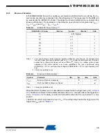
The voltage reference has a start-up time that may influence the way it should be used. The
start-up time is given in
. To save power, the reference is not always turned on. The
reference is on during the following situations:
1.
When the BOD is enabled (by programming the BODLEVEL [2..0] Fuse).
2.
When the bandgap reference is connected to the Analog Comparator (by setting the
ACBG bit in ACSR).
3.
When the ADC is enabled.
4.
When the DAC is enabled.
Thus, when the BOD is not enabled, after setting the ACBG bit or enabling the ADC or the DAC,
the user must always allow the reference to start up before the output from the Analog Compar-
ator or ADC or DAC is used. To reduce power consumption in Power-down mode, the user can
avoid the three conditions above to ensure that the reference is turned off before entering
Power-down mode.
9.1.2
Voltage Reference Characteristics
Note:
1. Values are guidelines only.
9.2
Watchdog Timer
AT90PWM2/2B/3/3B has an Enhanced Watchdog Timer (WDT). The main features are:
•
Clocked from separate On-chip Oscillator
•
3 Operating modes
– Interrupt
– System Reset
Table 9-4.
Internal Voltage Reference Characteristics
Symbol
Parameter
Condition
Min.
Typ.
Max.
Units
V
BG
Bandgap reference voltage
1.1
V
t
BG
Bandgap reference start-up time
40
µs
I
BG
Bandgap reference current
consumption
15
µA


