165
4317I–AVR–01/08
AT90PWM2/3/2B/3B
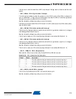
update of the PSC internal registers will be done at the end of the PSC cycle if the Output Com-
pare Register RB has been the last written.
When set, this bit prevails over LOCK (bit 5)
• Bit 5 – PLOCKn: PSC n Lock
When this bit is set, the Output Compare Registers RA, RB, SA, SB, the Output Matrix POM2
and the PSC Output Configuration PSOCn can be written without disturbing the PSC cycles.
The update of the PSC internal registers will be done if the LOCK bit is released to zero.
• Bit 4:3 – PMODEn1: 0: PSC n Mode
Select the mode of PSC.
• Bit 2 – POPn: PSC n Output Polarity
If this bit is cleared, the PSC outputs are active Low.
If this bit is set, the PSC outputs are active High.
• Bit 1 – PCLKSELn: PSC n Input Clock Select
This bit is used to select between CLKPF or CLKPS clocks.
Set this bit to select the fast clock input (CLKPF).
Clear this bit to select the slow clock input (CLKPS).
• Bit 0 – POME2: PSC 2 Output Matrix Enable (PSC2 only)
Set this bit to enable the Output Matrix feature on PSC2 outputs. See
When Output Matrix is used, the PSC n Output Polarity POPn has no action on the outputs.
16.25.11 PSC 0 Control Register – PCTL0
Table 16-13. PSC n Mode Selection
PMODEn1
PMODEn0
Description
0
0
One Ramp Mode
0
1
Two Ramp Mode
1
0
Four Ramp Mode
1
1
Center Aligned Mode
Bit
7
6
5
4
3
2
1
0
PPRE01
PPRE00
PBFM0
PAOC0B
PAOC0A
PARUN0
PCCYC0
PRUN0
PCTL0
Read/Write
R/W
R/W
R/W
R/W
R/W
R/W
R/W
R/W
Initial Value
0
0
0
0
0
0
0
0


