286
4317I–AVR–01/08
AT90PWM2/3/2B/3B
25.8
Parallel Programming
25.8.1
Enter Programming Mode
The following algorithm puts the device in Parallel (High-voltage) > Programming mode:
1.
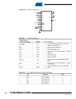
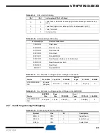
Set Prog_enable pins listed in Table 25-8. to “0000”, RESET pin to “0” and Vcc to 0V.
2.
Apply 4.5 - 5.5V between VCC and GND. Ensure that Vcc reaches at least 1.8V within
the next 20µs.
3.
Wait 20 - 60µs, and apply 11.5 - 12.5V to RESET.
4.
Keep the Prog_enable pins unchanged for at least 10µs after the High-voltage has been
applied to ensure the Prog_enable Signature has been latched.
5.
Wait at least 300µs before giving any parallel programming commands.
6.
Exit Programming mode by power the device down or by bringing RESET pin to 0V.
If the rise time of the Vcc is unable to fulfill the requirements listed above, the following alterna-
tive algorithm can be used.
1.
Set Prog_enable pins listed in Table 25-8. to “0000”, RESET pin to “0” and Vcc to 0V.
2.
Apply 4.5 - 5.5V between VCC and GND.
3.
Monitor Vcc, and as soon as Vcc reaches 0.9 - 1.1V, apply 11.5 - 12.5V to RESET.
4.
Keep the Prog_enable pins unchanged for at least 10µs after the High-voltage has been
applied to ensure the Prog_enable Signature has been latched.
5.
Wait until Vcc actually reaches 4.5 -5.5V before giving any parallel programming
commands.
6.
Exit Programming mode by power the device down or by bringing RESET pin to 0V.
25.8.2
Considerations for Efficient Programming
The loaded command and address are retained in the device during programming. For efficient
programming, the following should be considered.
•
The command needs only be loaded once when writing or reading multiple memory
locations.
•
Skip writing the data value 0xFF, that is the contents of the entire EEPROM (unless the
EESAVE Fuse is programmed) and Flash after a Chip Erase.
•
Address high byte needs only be loaded before programming or reading a new 256 word
window in Flash or 256 byte EEPROM. This consideration also applies to Signature bytes
reading.
25.8.3
Chip Erase
The Chip Erase will erase the Flash and EEPROM
memories plus Lock bits. The Lock bits are
not reset until the program memory has been completely erased. The Fuse bits are not
ch ange d. A Ch ip Erase m ust be pe rfo rm ed before the Flash and/o r EEPROM are
reprogrammed.
Note:
1. The EEPRPOM memory is preserved during Chip Erase if the EESAVE Fuse is programmed.
Load Command “Chip Erase”
1.
Set XA1, XA0 to “10”. This enables command loading.
2.
Set BS1 to “0”.
3.
Set DATA to “1000 0000”. This is the command for Chip Erase.
4.
Give XTAL1 a positive pulse. This loads the command.
5.
Give WR a negative pulse. This starts the Chip Erase. RDY/BSY goes low.


