293
4317I–AVR–01/08
AT90PWM2/3/2B/3B
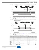
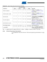
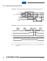
Figure 25-8. Parallel Programming Timing, Loading Sequence with Timing Requirements
Note:
1. The timing requirements shown in
(i.e., t
DVXH
, t
XHXL
, and t
XLDX
) also apply to load-
ing operation.
Figure 25-9. Parallel Programming Timing, Reading Sequence (within the Same Page) with
Timing Requirements
Note:
1. The timing requirements shown in
(i.e., t
DVXH
, t
XHXL
, and t
XLDX
) also apply to read-
ing operation.
Table 25-14. Parallel Programming Characteristics, V
CC
= 5V ± 10%
Symbol
Parameter
Min
Typ
Max
Units
V
PP
Programming Enable Voltage
11.5
12.5
V
I
PP
Programming Enable Current
250
μ
A
t
DVXH
Data and Control Valid before XTAL1 High
67
ns
t
XLXH
XTAL1 Low to XTAL1 High
200
ns
t
XHXL
XTAL1 Pulse Width High
150
ns
t
XLDX
Data and Control Hold after XTAL1 Low
67
ns
t
XLWL
XTAL1 Low to WR Low
0
ns
XTAL1
PAGEL
t
PLXH
XLXH
t
t
XLPH
ADDR0 (Low Byte)
DATA (Low Byte)
DATA (High Byte)
ADDR1 (Low Byte)
DATA
BS1
XA0
XA1
LOAD ADDRESS
(LOW BYTE)
LOAD DATA
(LOW BYTE)
LOAD DATA
(HIGH BYTE)
LOAD DATA
LOAD ADDRESS
(LOW BYTE)
XTAL1
OE
ADDR0 (Low Byte)
DATA (Low Byte)
DATA (High Byte)
ADDR1 (Low Byte)
DATA
BS1
XA0
XA1
LOAD ADDRESS
(LOW BYTE)
READ DATA
(LOW BYTE)
READ DATA
(HIGH BYTE)
LOAD ADDRESS
(LOW BYTE)
t
BVDV
t
OLDV
t
XLOL
t
OHDZ


