CDJ-800MK2
97
5
6
7
8
5
6
7
8
C
D
F
A
B
E
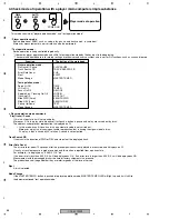
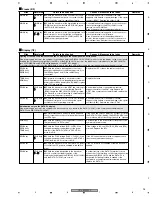
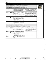
Audio output
Sites
Waveforms
Points to be checked
Causes & Measures to be taken
Remarks
No audio signal is output.
If a signal waveform is normally output from the digital output terminal (JA802), the AUDIO DSP (IC701) is judged to be normal. In
such a case, the problem exists at the subsequent stages of the AUDIO DSP output. During CD playback, first check the analog
output terminal (JA801) then the previous stages. Be sure to carefully check for solder fractures at the phono plug.
JACK Assy
z
Check the waveform of the audio output signal
at the analog output terminal (JA801).
Check if the audio signal is not output from L and
R channels, or only from one channel.
JACK Assy
x
Check if the digital audio signal is output from
the digital output terminal (JA802).
If the digital audio signal is also not output, the
AUDIO DSP (IC701) Assy is defective. See Step
v
in "No digital output."
JACK Assy
JACK Assy
c
Check the waveform at the L4 and R4 Test
Lands near analog output terminal (JA801).
If the audio signal is output from those points, a
solder fracture of the phono plug or chip fracture
on the audio line is suspected. Soldering touchup
is needed.
JACK Assy
SECB Assy
v
Check if 8 V and -7 V power are supplied to
the OP AMP (IC801).
If the power is not supplied, check the cable
connection of the power line.
JACK Assy
b
Check the waveform at the L1 and R1 Test
Lands on the OP AMP (IC801).
MAIN Assy
MAIN Assy
n
Check the waveform at the Lch and Rch Test
Lands near C705/C706.
If the audio signal is output at the point, audio
muting may remain activated. During CD
playback, check if the logical state of the signal
at Pin 4 of CN801 is low.
MAIN Assy
m
Check if 5 V power is supplied to the DAC
(IC702).
If the power is not supplied, check the cable
connection of the power line.
MAIN Assy
MAIN Assy
,
Check the waveform at the 11M Test Land,
referring to the waveform photo, to confirm that
the clock input to the DAC (IC702) is normal.
An unstable waveform or extremely low level
suggests loose connection of the clock terminal
on the AUDIO DSP.
MAIN Assy
MAIN Assy
to
.
Check the points (DACLRCK, DACDATA,
DACBCK) designated in the waveform photo to
confirm if the procedures of the communication
between the DAC (IC702) and AUDIO DSP
(IC701) are normal.
An unstable waveform suggests loose connection
output terminals on the AUDIO DSP or chip
fracture on the line.
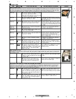
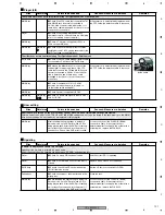
Audio performance is poor.
As grounding to the chassis is poor with this model, audio performance is largely affected if the specify screws are not tightened
with the standard torque.
z
Check if the screw that secures the bottom
plate and is located near the plug is a screw with
a projection (BBT).
Replace with a BBT screw if the original screw is
not BBT.
x
Check if the two screws that secure the
bottom plate, including the above-mentioned
screw with a projection, are firmly secured.
If the screws are loosely tightened, retighten the
screws with the standard torque.
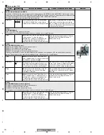
Poor S/N ratio at the intervals of no sound, such as between musical pieces
The S/N ratio is poor at the intervals of no sound, such as between musical pieces and at the time of power on, because audio
muting is not activated. Possible causes are zero-data detection signals not output from the DAC (IC702) or a defective audio
muting circuit. The following checks must be performed during CD playback.
MAIN Assy
MAIN Assy
z
Check the waveform at the terminal (Pin 21)
for zero-data detection on the DAC (IC702). If the
level is low between musical pieces and at the
time of power on and high during CD playback,
the terminal is normal.
If inversion of the logical state of signals is not
performed, loose connection of Pin 21 on the
DAC is most likely. Soldering touchup is needed.
MAIN Assy
MAIN Assy
x
Check the waveform at Pin 6 of CN701. If the
level is high between musical pieces and at the
time of power on and low during CD playback,
the terminal is normal.
If audio muting remains deactivated, check chip
fracture on the line or cable connection.
JA802
JA801
BBZ
BBT
40
45
35
41
43
44
46
Содержание CDJ-800MK2
Страница 27: ...CDJ 800MK2 27 5 6 7 8 5 6 7 8 C D F A B E MODE MODE 3 3 A 27 24 26 19 36 ...
Страница 29: ...CDJ 800MK2 29 5 6 7 8 5 6 7 8 C D F A B E Data PANEL DATA Digital A 2 3 3 3 A 3 3 A 23 ...
Страница 119: ...CDJ 800MK2 119 5 6 7 8 5 6 7 8 C D F A B E SCF5249LAG140 MAIN ASSY IC301 32 bit RISC MPU Block Diagram ...
Страница 130: ...CDJ 800MK2 130 1 2 3 4 1 2 3 4 C D F A B E Pin Function ...
Страница 135: ...CDJ 800MK2 135 5 6 7 8 5 6 7 8 C D F A B E Pin Function ...
Страница 138: ...CDJ 800MK2 138 1 2 3 4 1 2 3 4 C D F A B E PE8001A MAIN ASSY IC702 DAC IC Pin Arrangement Top view Block Diagram ...
Страница 139: ...CDJ 800MK2 139 5 6 7 8 5 6 7 8 C D F A B E Pin Function ...
Страница 143: ...CDJ 800MK2 143 5 6 7 8 5 6 7 8 C D F A B E ...
Страница 153: ...CDJ 800 7 5 6 7 8 5 6 7 8 C D F A B E ...
Страница 174: ...CDJ 800 28 1 2 3 4 1 2 3 4 C D F A B E 3 7 JFLB SLDB and JOGB ASSYS I JFLB ASSY DWG1565 I CN500 F ...
Страница 180: ...CDJ 800 34 1 2 3 4 1 2 3 4 C D F A B E ...
Страница 200: ...CDJ 800 54 1 2 3 4 1 2 3 4 C D F A B E 6 ADJUSTMENT There is no information to be shown in this chapter ...

