CDJ-800
3
5
6
7
8
5
6
7
8
C
D
F
A
B
E
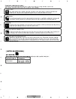
IMPORTANT
T H I S P I O N E E R A P PA R AT U S C O N TA I N S
LASER OF CLASS 1.
SERVICING OPERATION OF THE APPARATUS
S H O U L D B E D O N E B Y A S P E C I A L LY
INSTRUCTED PERSON.
LASER DIODE CHARACTERISTICS
MAXIMUM OUTPUT POWER: 5 mW
WAVELENGTH: 780
–
785 nm
WARNING !
The AEL(accessible emission level) of the laser power output is less then
CLASS 1
but the laser component is capable of emitting radiation exceeding the limit for
CLASS 1.
A specially instructed person should servicing operation of the apparatus.
Additional Laser Caution
1. Laser Interlock Mechanism
The position of the switch (S1901) for detecting loading
completion is detected by the system microprocessor, and
the design prevents laser diode oscillation when the switch
is not in LPS1 terminal side (when the mechanism is not
clamped and LPS1 signal is high level.) Thus, the interlock
will no longer function if the switch is deliberately set to LPS1
terminal side. ( if LPS1 signal is low level ).
In the test mode
∗
the interlock mechanism will not function.
Laser diode oscillation will continue, if pin 9 of TA2153FN
(IC118)on the MAIN ASSY is connected to GND,
or pin 10 of IC118 (LDON) is connected to low level
(ON), or else the terminals of Q110 are shorted to each
other (fault condition).
2. When the cover is opened, close viewing of the objective
lens with the naked eye will cause exposure to a Class 1
laser beam.
∗
: Refer to page 53.
CDJ-800 WYXJ : Types Only
Printed on the Bottom Plate
Bottom Plate
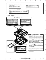
LABEL CHECK
Содержание CDJ-800MK2
Страница 27: ...CDJ 800MK2 27 5 6 7 8 5 6 7 8 C D F A B E MODE MODE 3 3 A 27 24 26 19 36 ...
Страница 29: ...CDJ 800MK2 29 5 6 7 8 5 6 7 8 C D F A B E Data PANEL DATA Digital A 2 3 3 3 A 3 3 A 23 ...
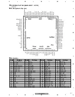
Страница 119: ...CDJ 800MK2 119 5 6 7 8 5 6 7 8 C D F A B E SCF5249LAG140 MAIN ASSY IC301 32 bit RISC MPU Block Diagram ...
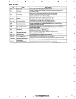
Страница 130: ...CDJ 800MK2 130 1 2 3 4 1 2 3 4 C D F A B E Pin Function ...
Страница 135: ...CDJ 800MK2 135 5 6 7 8 5 6 7 8 C D F A B E Pin Function ...
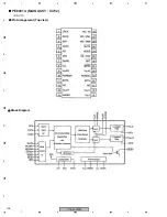
Страница 138: ...CDJ 800MK2 138 1 2 3 4 1 2 3 4 C D F A B E PE8001A MAIN ASSY IC702 DAC IC Pin Arrangement Top view Block Diagram ...
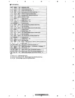
Страница 139: ...CDJ 800MK2 139 5 6 7 8 5 6 7 8 C D F A B E Pin Function ...
Страница 143: ...CDJ 800MK2 143 5 6 7 8 5 6 7 8 C D F A B E ...
Страница 153: ...CDJ 800 7 5 6 7 8 5 6 7 8 C D F A B E ...
Страница 174: ...CDJ 800 28 1 2 3 4 1 2 3 4 C D F A B E 3 7 JFLB SLDB and JOGB ASSYS I JFLB ASSY DWG1565 I CN500 F ...
Страница 180: ...CDJ 800 34 1 2 3 4 1 2 3 4 C D F A B E ...
Страница 200: ...CDJ 800 54 1 2 3 4 1 2 3 4 C D F A B E 6 ADJUSTMENT There is no information to be shown in this chapter ...

