CDJ-800MK2
95
5
6
7
8
5
6
7
8
C
D
F
A
B
E
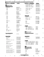
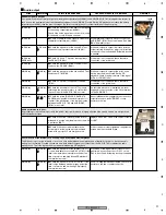
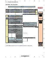
Display (1/2)
Sites
Waveforms
Points to be checked
Causes & Measures to be taken
Remarks
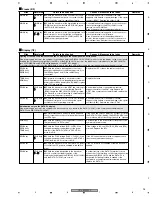
Lighting of the LEDs and indications and the FL display on the control panel do not function.
If the power supply is normal, this symptom is caused by a defective DISPLAY MPU (IC501,) which controls the display on the control panel,
including the FL indication and lighting of the LEDs. (If the DISPLAY MPU is normal, the indications of internal data on the DISPLAY MPU,
such as POWERON and E-8709, will be displayed on the DATA-FL display.)
To confirm that the core block of the MAIN Assy is normal, play back a CD without using the control panel and check the audio output.
DFLB Assy
SECB Assy
REGB Assy
z
Check the power to be supplied to the control
panel, paying attention to the following points: (1) Is
the ICP damaged?, and (2) Are cables firmly
connected?
Replace the ICP or check the cable connections.
TRNS Assy
ACIN Assy
x
If power is not supplied to any power system,
check the primary source. Inappropriate commercial
power input or blown primary fuse (FU8001) or glass
fuse (T21) are possible.
Replace the fuses.
DFLB Assy
DFLB Assy
c
Check the waveform of the XRST line, referring to
the waveform photo, to confirm that the Reset IC
(IC502) resets the DISPLAY MPU (IC501) properly.
The Reset IC is normal if resetting is canceled about
70 msec after the power is turned on.
Abnormal delay time or an unstable waveform
suggests fracture of the C507 chip. Replace the
C507. If the symptom is not ameliorated, replace the
IC502.
DFLB Assy
DFLB Assy
v
Check the waveform at Pin 12 of IC501, referring
to the waveform photo, to confirm that the crystal
oscillation circuit is operating normally.
An unstable waveform or extremely low level
suggests chip fracture or partial damage of the crystal
oscillator (X501). Replace the chip or X501.
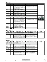
No indication only on the DATA-FL display
If the power supply is normal, this symptom can be caused only by a failure in the DATA-FL (V501) or the communication between the
DATA-FL and DISPLAY MPU (IC501).
z
Enter Display Check mode of Service mode and
check if other keys on the control panel function and if
the LEDs light.
If the LEDs and JOG-FL (V601) do not light, nor does
the DATA-FL (V501) display, the DISPLAY MPU that
controls those will not function properly. See "Lighting
ACIN Assy
x
Check the setting of the voltage selector switch (on
the rear panel). (for RLF model)
Set the switch to the position that corresponds to the
commercial power source.
DFLB Assy
SECB Assy
TRNS Assy
c
Check the Vload voltage (VLD, VLDD). If the
voltage measured at the periphery of the power
terminal of the DATA-FL (V501) is 29.3 V DC or
more, it is OK.
If the voltage is 0 V, the ICPs (IC25, IC58, and IC59)
are fried. Replace the ICPs.
DFLB Assy
DFLB Assy
v
Check the FLAC voltage (FLAC1, FLAC2). If the
voltage measured at the both ends of the DATA-FL
(V501) lead is 4 V AC or more, it is OK.
If the AC current waveform does not appear, check
the connection between the Assys.
DFLB Assy
b
Check the waveform at Pin 46 of DATA-FL (V501),
to confirm that 5 V power is supplied to the built-in
driver.
If the 5 V power is not supplied, soldering touchup is
needed.
DFLB Assy
DFLB Assy
to
n
Check the points designated in the waveform
photo to confirm that the procedures of the
communication between the DISPLAY MPU (IC501)
and the DATA-FL (V501) are normal.
A solder fracture of the DATA-FL terminal or loose
connection of the terminals on the communication line
between the DISPLAY MPU and the DATA-FL is
suspected. Soldering touchup is needed. If the
symptom is not ameliorated after soldering touchup,
replace the DATA-FL.
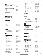
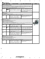
Freeze (2/2)
Sites
Waveforms
Points to be checked
Causes & Measures to be taken
Remarks
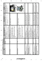
MAIN Assy
MAIN Assy
ç
Check the waveform at the designated point on the
PRGM line, to confirm that the MPU (IC301) resets
the FPGA (IC302) properly.
An unstable waveform suggests loose connection of
the output terminal of the MPU (IC301) or chip
fracture on the PRGM line.
Even if the waveform at the designated point is
MAIN Assy
MAIN Assy
to
√
Check the waveform at the point designated on the
waveform photo, to confirm that the configuration
procedures between the MPU (IC301) and FPGA
(IC302) are properly performed.
An unstable waveform suggests loose connection of
the output terminal or chip fracture.
Even if the waveform at the designated point is
normal, there may be poor contact of connectors in
downstream lines. Resolder the output connectors,
19
23
30
49
72
74
54
57
MAIN Assy
MAIN Assy
≈
Check the waveform at the CPU16M Test Land,
referring to the waveform photo, to confirm that the
crystal oscillation circuit is operating normally.
An unstable waveform or extremely low level
suggests chip fracture or partial damage of the crystal
oscillator (X301). Replace the chip or X301.
71
Содержание CDJ-800MK2
Страница 27: ...CDJ 800MK2 27 5 6 7 8 5 6 7 8 C D F A B E MODE MODE 3 3 A 27 24 26 19 36 ...
Страница 29: ...CDJ 800MK2 29 5 6 7 8 5 6 7 8 C D F A B E Data PANEL DATA Digital A 2 3 3 3 A 3 3 A 23 ...
Страница 119: ...CDJ 800MK2 119 5 6 7 8 5 6 7 8 C D F A B E SCF5249LAG140 MAIN ASSY IC301 32 bit RISC MPU Block Diagram ...
Страница 130: ...CDJ 800MK2 130 1 2 3 4 1 2 3 4 C D F A B E Pin Function ...
Страница 135: ...CDJ 800MK2 135 5 6 7 8 5 6 7 8 C D F A B E Pin Function ...
Страница 138: ...CDJ 800MK2 138 1 2 3 4 1 2 3 4 C D F A B E PE8001A MAIN ASSY IC702 DAC IC Pin Arrangement Top view Block Diagram ...
Страница 139: ...CDJ 800MK2 139 5 6 7 8 5 6 7 8 C D F A B E Pin Function ...
Страница 143: ...CDJ 800MK2 143 5 6 7 8 5 6 7 8 C D F A B E ...
Страница 153: ...CDJ 800 7 5 6 7 8 5 6 7 8 C D F A B E ...
Страница 174: ...CDJ 800 28 1 2 3 4 1 2 3 4 C D F A B E 3 7 JFLB SLDB and JOGB ASSYS I JFLB ASSY DWG1565 I CN500 F ...
Страница 180: ...CDJ 800 34 1 2 3 4 1 2 3 4 C D F A B E ...
Страница 200: ...CDJ 800 54 1 2 3 4 1 2 3 4 C D F A B E 6 ADJUSTMENT There is no information to be shown in this chapter ...

