CDJ-800MK2
94
1
2
3
4
1
2
3
4
C
D
F
A
B
E
7.1.3 TROBLE SHOOTING
Points to be checked beforehand and a note :
• When a failure judgment of the ICP (Micro Fuse) is performed using a tester, be sure to judge according to the resistance values. If a simplified measurement
method, such as Short-circuit Check mode, is used for testing, a partially-damaged ICP cannot be detected.
• The ICP is very sensitive. First, check the power line to verify that the placed ICP is not damaged.
• Defective soldering of surface mount devices may have caused a problem. Check if the symptom changes when you press the corresponding surface mount
device with a finger.
• For the address-bus and data-bus lines on the MAIN Assy, the dump (serial) resistance is never used.
Note :
The numbers for the waveform photos are identical to those for the schematic diagrams and board diagrams.
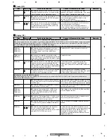
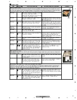
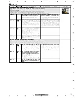
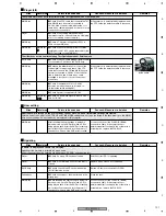
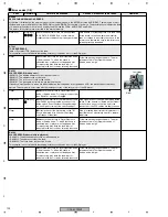
Freeze (1/2)
Sites
Waveforms
Points to be checked
Causes & Measures to be taken
Remarks
E8709 error
If the power supply is normal, this symptom is caused either by a defective core block of the MAIN Assy or a failure in
communication between the DISPLAY MPU (IC501) and MAIN Assy. A defective core block means that the processes up to the
FPGA (IC302) configuration have not been completed. In a case of a failure in the communication line, the core block is normal. In
either case, no error indication is displayed on the control panel because the E8709 error code is sent to the DATA-FL display by
the DISPLAY MPU itself.
Note:
The core block comprises 4 main ICs: MPU (IC301), SDRAM (IC303), FLASH (IC300), and FPGA (IC302).
z
Play back a CD.
Check if the audio signal is output from the
analog output terminal (JA801).
If the audio signal is output, the core block is OK.
The cause is a failure in communication between
the DISPLAY MPU and the MAIN Assy. On the
contrary, if the CD cannot be played, the core
block is in failure. Proceed to Step
b
.
DFLB Assy
SECB Assy
x
Disconnect then reconnect the FFC cable
between the DFLB and SECB Assys, and that
between the SECB and MAIN Assys to check if
the symptom is ameliorated.
If the symptom is ameliorated, loose connection
of the FFC cable is the cause.
Unit
c
Disconnect then reconnect the FFC cable
between the MAIN and JACK Assys and the
cable with connectors that connects the JACK
and SECB Assys to check if the symptom is
ameliorated. Also check for the 5 V power line,
including loose connection of the connectors.
DFLB Assy
SECB Assy
MAIN Assy
DFLB Assy
to
v
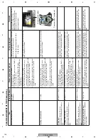
Check the waveform at the points (TSCLK,
TSDO, TSDI, and TSCS) designated in the
waveform photo to confirm that the
communication line between the DISPLAY MPU
(IC301) and FPGA (IC302) is normal.
If the waveform is unstable or extremely low in
level, loose connection of the output terminals or
connectors on the line, chip fracture, poor power
supply to IC308, or partial damage of IC308 may
be the cause. Replace IC308 and check the
connections.
If 5 V power is not supplied to the DAC (IC702),
the 3-wire serial signal level between the DAC
and the MPU is lowered, because the DAC is not
started, which will lead to a failure in starting of
the FPGA (the loading motor rattles). Repair the
5 V power line.
MAIN Assy
m
Check if the soldered portion of IC311 on the
CLK line is lifted off the board.
Note: It has been found that the cell and the part
are not compatible. With the Assys of the lots
before the modification, defective mounting may
have occurred.
If the defective mounting of IC311 is the cause,
"POWER ON" is displayed for a while, a rattle is
generated from the player, then E8709 error is
indicated. A disc cannot be loaded in the player.
b
5 Deployment of the data that had been
written in the flash memory (IC300) into the
SRAM built into the MPU (IC301) may have
failed. Check that the voltage at TP19 is 0 V.
If the waveform at TP19 continuously fluctuates,
deployment of the data failed. A checksum error
of the SRAM built into the MPU (IC301) was
generated. Check the mounting status of IC301.
n
6 Deployment of the program and data that
had been written in the flash memory (IC300)
into the SDRAM (IC303) may have failed. Check
that the voltage at TP30 is 0 V.
If the waveform at TP30 continuously fluctuates,
deployment of the program and data failed. A
checksum error of the SDRAM (IC303) was
generated. Check the mounting status of IC303.
MAIN Assy
,
Check if the soldered portion of IC312 on the
PRGM line is lifted off the board.
Note: It has been found that the cell and the part
are not compatible. With the Assys of the lots
before the modification, defective mounting may
have occurred.
If the defective mounting of IC312 is the cause,
"POWER ON" is displayed for a while, then
E8709 error is indicated. A disc cannot be loaded
in the player.
Replace the ICP or check the cable connections.
MAIN Assy
SECB Assy
REGB Assy
.
Check the power system for the core block,
paying attention to the following points: (1) Is the
ICP damaged?, and (2) Are cables firmly
connected?
TRNS Assy
ACIN Assy
/
If power is not supplied to any power system,
check the primary source. Inappropriate
commercial power input or blown primary fuse
(FU8001) or transformer fuse (T21) may be the
cause.
Replace the fuses.
MAIN Assy
MAIN Assy
Ω
Check the waveform at the RST Test Land,
referring to the waveform photo, to confirm that
the Reset IC (IC304) resets the MPU (IC301)
properly. The Reset IC is normal if resetting is
canceled about 70 msec after the power is
turned on.
Abnormal delay time or an unstable waveform
suggests fracture of the C303 chip. Replace the
C303. If the symptom is not ameliorated, replace
the IC304.
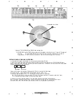
Control panel
4
7
18
Содержание CDJ-800MK2
Страница 27: ...CDJ 800MK2 27 5 6 7 8 5 6 7 8 C D F A B E MODE MODE 3 3 A 27 24 26 19 36 ...
Страница 29: ...CDJ 800MK2 29 5 6 7 8 5 6 7 8 C D F A B E Data PANEL DATA Digital A 2 3 3 3 A 3 3 A 23 ...
Страница 119: ...CDJ 800MK2 119 5 6 7 8 5 6 7 8 C D F A B E SCF5249LAG140 MAIN ASSY IC301 32 bit RISC MPU Block Diagram ...
Страница 130: ...CDJ 800MK2 130 1 2 3 4 1 2 3 4 C D F A B E Pin Function ...
Страница 135: ...CDJ 800MK2 135 5 6 7 8 5 6 7 8 C D F A B E Pin Function ...
Страница 138: ...CDJ 800MK2 138 1 2 3 4 1 2 3 4 C D F A B E PE8001A MAIN ASSY IC702 DAC IC Pin Arrangement Top view Block Diagram ...
Страница 139: ...CDJ 800MK2 139 5 6 7 8 5 6 7 8 C D F A B E Pin Function ...
Страница 143: ...CDJ 800MK2 143 5 6 7 8 5 6 7 8 C D F A B E ...
Страница 153: ...CDJ 800 7 5 6 7 8 5 6 7 8 C D F A B E ...
Страница 174: ...CDJ 800 28 1 2 3 4 1 2 3 4 C D F A B E 3 7 JFLB SLDB and JOGB ASSYS I JFLB ASSY DWG1565 I CN500 F ...
Страница 180: ...CDJ 800 34 1 2 3 4 1 2 3 4 C D F A B E ...
Страница 200: ...CDJ 800 54 1 2 3 4 1 2 3 4 C D F A B E 6 ADJUSTMENT There is no information to be shown in this chapter ...

