2
1
2
3
4
1
2
3
4
C
D
F
A
B
E
CDJ-800MK2
CONTRAST OF PCB ASSEMBLIES
AC IN ASSY
F
E
Mark
Symbol and Description
Part No.
Remarks
DWR1430
DWR1429
AC Inlet 1P
XKP3042
XKP3041
DWR1429 and DWR1430 are constructed the same except for the following :
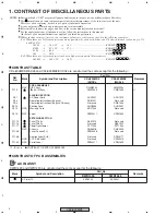
1. CONTRAST OF MISCELLANEOUS PARTS
j
p
f
y
For the applying amount of lubricants or glue, follow the instructions in this manual.
(In the case of no amount instructions, apply as you think it appropriate.)
Parts marked by "NSP" are generally unavailable because they are not in our Master Spare Parts List.
The mark found on some component parts indicates the importance of the safety factor of the part.
Therefore, when replacing, be sure to use parts of identical designation.
Screws adjacent to mark on product are used for disassembly.
Reference Nos. indicate the pages and Nos. in the service manual for the base model.
NOTES:
•
When ordering resistors, first convert resistance values into code form as shown in the following examples.
Ex.1 When there are 2 effective digits (any digit apart from 0), such as 560 ohm and 47k ohm (tolerance is shown by J=5%,
and K=10%).
560
Ω
→
56
×
10
1
→
561 ........................................................ RD1/4PU
5
6
1
J
47k
Ω
→
47
×
10
3
→
473 ........................................................ RD1/4PU
4
7
3
J
0.5
Ω
→
R50 ..................................................................................... RN2H
R
5
0
K
1
Ω
→
1R0 ..................................................................................... RS1P
1
R
0
K
Ex.2 When there are 3 effective digits (such as in high precision metal film resistors).
5.62k
Ω →
562
×
10
1
→
5621 ...................................................... RN1/4PC
5
6
2
1
F
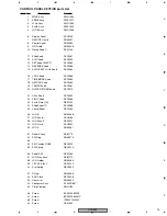
CONTRAST TABLE
Ref.
Part No.
No.
Mark
Symbol and Description
CDJ-800MK2
CDJ-800MK2
Remarks
/KUCXJ
/WAXJ5
PCB ASSEMBLIES
NSP
DISP Assy
DWM2234
DWM2233
P11-2
AC IN Assy
DWR1430
DWR1429
∗
1
PACKING SECTION
P9-1
AC Power Cord
ADG7021
ADG7079
P9-4
Operating Instructions (English)
DRB1401
Not used
P9-4
Operating Instructions (English, Chinese)
Not used
DRB1403
P9-12
Packing Case
DHG2595
DHG2597
P9-13
NSP
Warranty Card
ARY7043
Not used
P9-14
NSP
Label
DRW2311
VRW1629
EXTERIOR SECTION
P11-10
Fuse(T1.6 A)
AEK7075
Not used
P11-10
Fuse(T0.8 A)
Not used
REK1021
P11-17
Power Transfomer
DTT1204
DTT1203
NSP
Chassis
DNK4518
DNK4520
P11-38
Laser Caution(7L)
DRW2308
Not used
P11-38
Caution Label(CHK)
Not used
DRW2177
NSP
CCC S&E Label
Not used
DRW2310
P11-39
NSP
Serial Label
DRW2311
VRW1629
CDJ-800MK2/WAXJ5 and CDJ-800MK2/KUCXJ are constructed the same except for the following :
∗
1 : Refer to “
7
CONTRAST OF PCB ASSEMBLIES ”
Содержание CDJ-800MK2
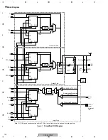
Страница 27: ...CDJ 800MK2 27 5 6 7 8 5 6 7 8 C D F A B E MODE MODE 3 3 A 27 24 26 19 36 ...
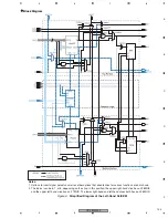
Страница 29: ...CDJ 800MK2 29 5 6 7 8 5 6 7 8 C D F A B E Data PANEL DATA Digital A 2 3 3 3 A 3 3 A 23 ...
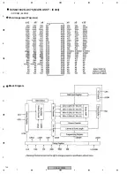
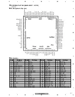
Страница 119: ...CDJ 800MK2 119 5 6 7 8 5 6 7 8 C D F A B E SCF5249LAG140 MAIN ASSY IC301 32 bit RISC MPU Block Diagram ...
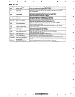
Страница 130: ...CDJ 800MK2 130 1 2 3 4 1 2 3 4 C D F A B E Pin Function ...
Страница 135: ...CDJ 800MK2 135 5 6 7 8 5 6 7 8 C D F A B E Pin Function ...
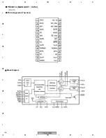
Страница 138: ...CDJ 800MK2 138 1 2 3 4 1 2 3 4 C D F A B E PE8001A MAIN ASSY IC702 DAC IC Pin Arrangement Top view Block Diagram ...
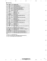
Страница 139: ...CDJ 800MK2 139 5 6 7 8 5 6 7 8 C D F A B E Pin Function ...
Страница 143: ...CDJ 800MK2 143 5 6 7 8 5 6 7 8 C D F A B E ...
Страница 153: ...CDJ 800 7 5 6 7 8 5 6 7 8 C D F A B E ...
Страница 174: ...CDJ 800 28 1 2 3 4 1 2 3 4 C D F A B E 3 7 JFLB SLDB and JOGB ASSYS I JFLB ASSY DWG1565 I CN500 F ...
Страница 180: ...CDJ 800 34 1 2 3 4 1 2 3 4 C D F A B E ...
Страница 200: ...CDJ 800 54 1 2 3 4 1 2 3 4 C D F A B E 6 ADJUSTMENT There is no information to be shown in this chapter ...

