NuMicro® NUC029LEE/NUC029SEE
32-bit Arm
®
Cortex
®
-M0 Microcontroller
Aug, 2018
Page
390
of
497
Rev 1.00
N
U
MICRO
®
N
UC02
9L
E
E
/N
UC029
S
E
E
T
E
CHN
ICA
L R
E
F
E
R
E
NC
E
M
A
NU
A
L
6.14.3 Basic Configuration
The basic configurations of I
2
C0 are as follows:
I
2
C0 pins are configured on GPA_MFP [9:8] register
Enable I
2
C0 clock by setting I2C0_EN (APBCLK [8])
Reset I
2
C0 controller by setting I2C0_RST(IPRSTC2 [8])
The basic configurations of I
2
C1 are as follows:
I
2
C1 pins are configured on GPE_MFP [11:10] register
Enable I
2
C1 clock by setting I2C1_EN( APBCLK [9])
Reset I
2
C1 controller by setting I2C1_RST (IPRSTC2 [9])
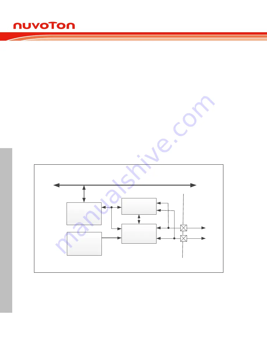
6.14.4 Block Diagram
The basic configurations of I
2
C are as follows:
Control Register
APB Interface
Bus Clock Control
Wakeup Control
Bus Protocol
Interface Control
I2Cn_SCL
I2Cn_SDA
Figure 6.14-1 I
2
C Controller Block Diagram
6.14.5 Functional Description
On I
2
C bus, data is transferred between a Master and a Slave. Data bits transfer on the
I2Cn_SCL and I2Cn_SDA lines are synchronously on a byte-by-byte basis. Each data byte is 8-
bit long. There is one I2Cn_SCL clock pulse for each data bit with the MSB being transmitted first,
and an acknowledge bit follows each transferred byte. Each bit is sampled during the high period


