


Chapter 3
Using the NI PXI-4204
3-22
ni.com
Other Application Documentation and Material
The following locations provide more information that you may find useful
when setting up or connecting signal sources or programming your
application.
•
LabVIEW Example Programs, available by selecting
Open»
Examples
from the opening screen. Most of the examples applicable
to the NI PXI-4204 are located in
Hardware Input and Output»
DAQmx»Analog Measurements
and
Hardware Input and
Output»DAQmx»Synchronization»Multi-Device
.
•
PXI-4204 Supported Properties
in the LabVIEW
VI, Function, &
How-To Help
.
•
Application Note 025:
Field Wiring and Noise Considerations for
Analog Signals
available at
ni.com
. Go to
ni.com/info
and enter
the info code
rdfwn3
.
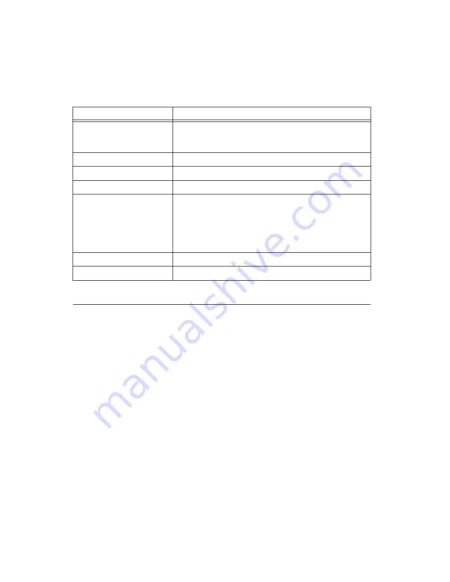
Configure Slave Triggering
DAQmx Trigger.vi
(Start Digital Edge) use
/MasterDevice/
ai/StartTrigger
as the source, substituting the master device
identifier for
MasterDevice
.
Start Slave Measurement(s)
DAQmx Start Task.vi
Start Master Measurement
DAQmx Start Task.vi
Read Measurement
DAQmx Read.vi
Continue Sampling
For continuous sampling, use a While Loop. You also need
to have set the sample mode to
Continuous Samples
in the
and
steps.
To do this, right-click the terminal of the
DAQmx Timing.vi
labeled
sample mode
and click
Create»Constant
. Click the
box that appears and select
Continuous Samples
.
Clear Master Task
DAQmx Clear Task.vi
Clear Slave Task
DAQmx Clear Task.vi
Table 3-5.
Synchronizing the NI PXI-4204 Using LabVIEW (Continued)
Flowchart Step
VI or Program Step


