Memory Maps
MVME162/D2
3-7
3
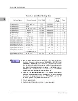
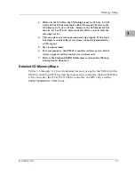
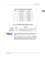
3. Writes to the LCSR in the VMEchip2 must be 32 bits. LCSR
writes of 8 or 16 bits terminate with a TEA signal. Writes to the
GCSR may be 8, 16 or 32 bits. Reads to the LCSR and GCSR
may be 8, 16 or 32 bits. Byte reads should be used to read the
interrupt vector.
4. This area does not return an acknowledge signal. If the local
bus timer is enabled, the access times out and is terminated by
a TEA signal.
5. Size is approximate.
6. Port commands to the 82596CA must be written as two 16-bit
writes: upper word first and lower word second.
7. Refer to the Flash and EPROM Interface section in the MCchip
description in Chapter 3.
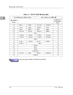
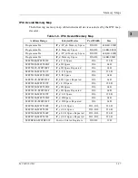
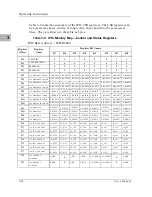
Detailed I/O Memory Maps
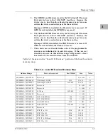
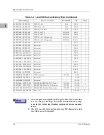
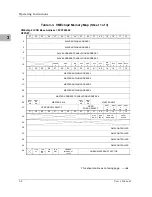
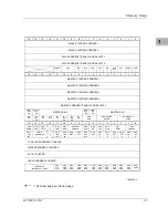
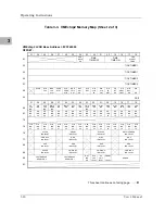
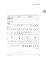
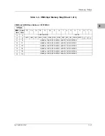
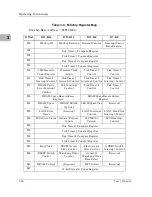
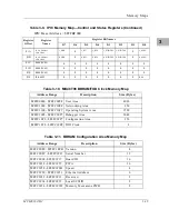
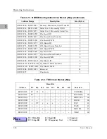
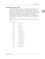
Tables 3-3 through 3-12 provide detailed memory maps for the VMEchip2, the
MCchip, the Zilog Z85230 serial communications controller, the Intel 82596CA
LAN controller, the NCR 53C710 SCSI controller, the IPIC chip, and the
MK48T08 BBRAM/TOD Clock.
Содержание MVME162
Страница 1: ...MVME162 Embedded Controller User s Manual MVME162 D2 ...
Страница 6: ......
Страница 10: ...x ...
Страница 12: ...xii ...
Страница 14: ...xiv ...
Страница 52: ...Hardware Preparation and Installation 2 26 MVME162 Embedded Controller User s Manual 2 ...
Страница 64: ...Operating Instructions 3 12 User s Manual 3 This page intentionally left blank ...
Страница 78: ...Operating Instructions 3 26 User s Manual 3 ...
Страница 92: ...Functional Description 4 14 User s Manual 4 Figure 4 1 MVME162 Main Module Block Diagram ...
Страница 94: ...Functional Description 4 16 User s Manual 4 Figure 4 2 Parity DRAM Mezzanine Module Block Diagram ...
Страница 106: ...Index IN 4 User s Manual I N D E X ...

