MVME162LX/D1IN-1
Index
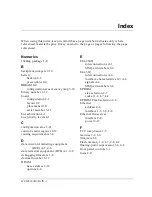
When using this index, keep in mind that a page number indicates only where
referenced material begins. It may extend to the page or pages following the page
referenced.
Numerics
162Bug package 1-8
B
backplane jumpers 2-10
battery
backup 4-2
precautions 4-4
BBRAM 4-4
configuration area memory map 3-19
binary number 1-12
board
configuration 2-1
layout 2-2
placement 2-10
serial number 3-21
bus arbitration 4-1
bus priority levels 4-1
C
configuration area 3-21
control/status register 2-12
cooling requirements 1-4
D
data circuit-terminating equipment
(DCE) A-1, 4-6
data terminal equipment (DTE) A-1, 4-6
debugging firmware 1-8
decimal number 1-12
DRAM
base address 2-12
options 4-4
E
EIA-232-D
interconnections A-1
SIM part numbers 2-4
EIA-530
interconnections A-4
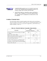
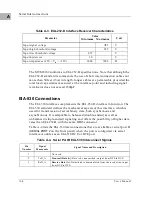
interface characteristics 4-7, A-6
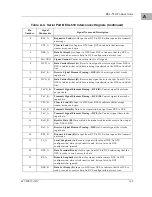
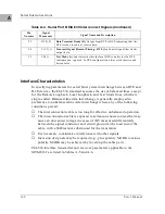
signals A-4
SIM part numbers 2-4
EPROM
size selection 2-7
socket 1-2, 1-7, 4-2
EPROM/Flash selection 2-8
Ethernet
address 4-8
interface 1-2, 1-8, 4-8
Ethernet transceiver
interface 2-13
power 2-13
F
FCC compliance 1-5
features 1-2, 1-6
firmware 1-8
Flash memory 1-2, 1-7, 2-8, 4-2
floating-point coprocessor 1-6, 4-2
front panel controls 3-1
fuses 2-13
Содержание MVME162
Страница 1: ...MVME162 Embedded Controller User s Manual MVME162 D2 ...
Страница 6: ......
Страница 10: ...x ...
Страница 12: ...xii ...
Страница 14: ...xiv ...
Страница 52: ...Hardware Preparation and Installation 2 26 MVME162 Embedded Controller User s Manual 2 ...
Страница 64: ...Operating Instructions 3 12 User s Manual 3 This page intentionally left blank ...
Страница 78: ...Operating Instructions 3 26 User s Manual 3 ...
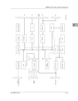
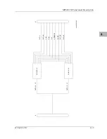
Страница 92: ...Functional Description 4 14 User s Manual 4 Figure 4 1 MVME162 Main Module Block Diagram ...
Страница 94: ...Functional Description 4 16 User s Manual 4 Figure 4 2 Parity DRAM Mezzanine Module Block Diagram ...
Страница 106: ...Index IN 4 User s Manual I N D E X ...

