MVME162 Functional Description
MVME162/D2
4-11
4
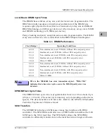
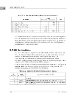
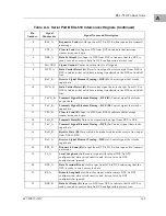
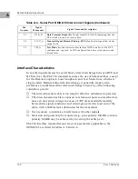
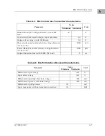
Local Bus to DRAM Cycle Times
The DRAM base address, array size, and device size are programmable. The
DRAM controller assumes an interleaved architecture if the DRAM size
requires eight physical devices (that is, when memory array size is 4MB and
DRAM technology is 4 Mbits per device; or when memory array size is 16MB
and DRAM technology is 16 Mbits per device.)
Parity checking and parity exception action is also programmable. The DRAM
array size and device size are initialized in the DRAM Space Size Register.
N
ote
TEA is the MC68040 bus error transaction signal. "With TEA"
indicates that a bus error cycle occurs if a DRAM parity error was
detected.
EPROM/Flash Cycle Times
The EPROM/Flash cycle time is programmable from 3 to 10 bus clocks/byte
(4 bytes = 12 to 40). (The actual cycle time may vary depending on the device
speed.) The data transfers are 32 bits wide. Refer to the MVME162 Embedded
Controller Programmer’s Reference Guide.
SCSI Transfers
The MVME162 includes an SCSI mass storage bus interface with DMA
controller. The SCSI DMA controller uses a FIFO buffer to interface the 8-bit
SCSI bus to the 32-bit local bus. The FIFO buffer allows the SCSI DMA
controller to efficiently transfer data to the local bus in four longword bursts.
Table 4-1. DRAM Performance
Clock Budget
Operating Conditions
4,2,2,2
Non-interleaved, read, 25 MHz, without TEA on parity error
4,1,1,1
Interleaved, read, 25 MHz, without TEA on parity error
5,3,3,3
Non-interleaved, read, 25 MHz, with TEA on parity error
5,2,2,2
Interleaved, read, 25 MHz, with TEA on parity error
3,2,2,2
Write, 25 MHz
5,3,3,3
Non-interleaved, read, 33 MHz, without TEA on parity error
5,2,2,2
Interleaved, read, 33 MHz, without TEA on parity error
6,4,4,4
Non-interleaved, read, 33 MHz, with TEA on parity error
6,3,3,3
Interleaved, read, 33 MHz, with TEA on parity error
4,2,2,2
Write, 33 MHz
Содержание MVME162
Страница 1: ...MVME162 Embedded Controller User s Manual MVME162 D2 ...
Страница 6: ......
Страница 10: ...x ...
Страница 12: ...xii ...
Страница 14: ...xiv ...
Страница 52: ...Hardware Preparation and Installation 2 26 MVME162 Embedded Controller User s Manual 2 ...
Страница 64: ...Operating Instructions 3 12 User s Manual 3 This page intentionally left blank ...
Страница 78: ...Operating Instructions 3 26 User s Manual 3 ...
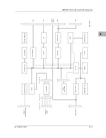
Страница 92: ...Functional Description 4 14 User s Manual 4 Figure 4 1 MVME162 Main Module Block Diagram ...
Страница 94: ...Functional Description 4 16 User s Manual 4 Figure 4 2 Parity DRAM Mezzanine Module Block Diagram ...
Страница 106: ...Index IN 4 User s Manual I N D E X ...

