Functional Description
4-12
User’s Manual
4
This reduces local bus usage by the SCSI device. Refer to the MCchip
Programming Model in the MVME162 Embedded Controller Programmer’s
Reference Guide.
The transfer rate of the DMA controller is 44MB/sec at 25 MHz with parity off
and interleaved DRAM and read cycles. Assuming a continuous transfer rate
of 5MB/sec on the SCSI bus, 12% of the local bus bandwidth is used by
transfers from the SCSI bus.
LAN DMA Transfers
The MVME162 includes a LAN interface with DMA controller. The LAN DMA
controller uses a FIFO buffer to interface the serial LAN bus to the 32-bit local
bus. The FIFO buffer allows the LAN DMA controller to efficiently transfer
data to the local bus.
The 82596CA does not execute MC68040 compatible burst cycles, therefore the
LAN DMA controller does not use burst transfers. Parity DRAM write cycles
require 3 clock cycles, and read cycles require 5 clock cycles with parity off and
6 clock cycles with parity on.
The transfer rate of the LAN DMA controller is 20MB/sec at 25 MHz with
parity off. Assuming a continuous transfer rate of 1MB/sec on the LAN bus,
5% of the local bus bandwidth is used by transfers from the LAN bus.
Remote Status and Control
The remote status and control connector, J4, is a 20-pin connector located
behind the front panel of the MVME162. It provides system designers with
flexibility in accessing critical indicator and reset functions. This allows a
system designer to construct a
RESET
/
ABORT
/LED panel that can be located
remotely from the MVME162.
Содержание MVME162
Страница 1: ...MVME162 Embedded Controller User s Manual MVME162 D2 ...
Страница 6: ......
Страница 10: ...x ...
Страница 12: ...xii ...
Страница 14: ...xiv ...
Страница 52: ...Hardware Preparation and Installation 2 26 MVME162 Embedded Controller User s Manual 2 ...
Страница 64: ...Operating Instructions 3 12 User s Manual 3 This page intentionally left blank ...
Страница 78: ...Operating Instructions 3 26 User s Manual 3 ...
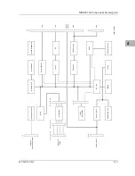
Страница 92: ...Functional Description 4 14 User s Manual 4 Figure 4 1 MVME162 Main Module Block Diagram ...
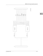
Страница 94: ...Functional Description 4 16 User s Manual 4 Figure 4 2 Parity DRAM Mezzanine Module Block Diagram ...
Страница 106: ...Index IN 4 User s Manual I N D E X ...

