


2BT
2-3-1
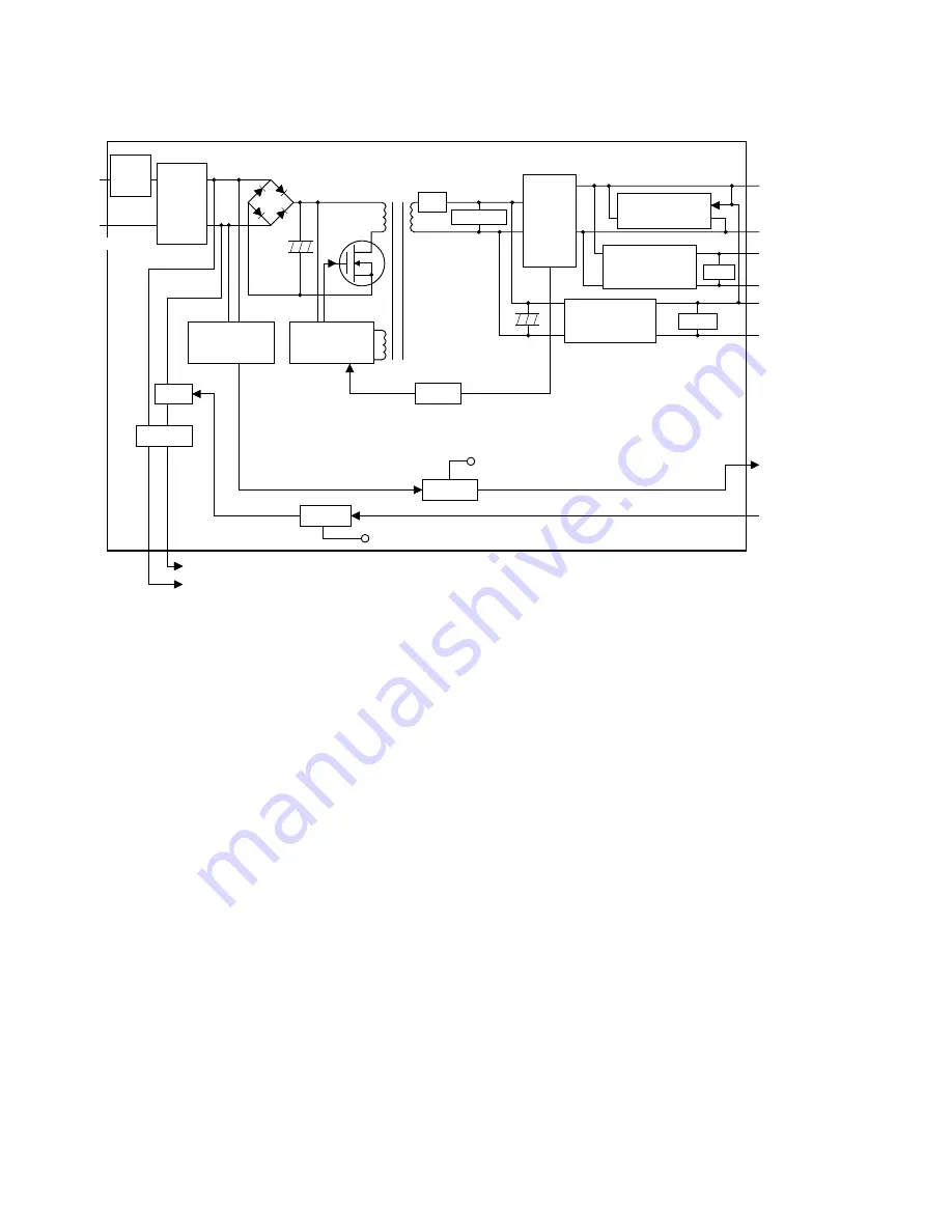
2-3-1 Power source PCB
Figure 2-3-1 Power source PCB block diagram
The power source PCB (PSPCB) is a switching regulator that converts an AC input to generate 24 V DC, 5.1 V DC and 12
V DC. It includes a noise filter circuit, a rectifier circuit, a switching regulator circuit, a 24 V DC output circuit, a 5 V DC output
circuit, a 12 V DC output circuit, a fixing heater control circuit and a zero-cross detection circuit.
The noise filter circuit consists mainly of a line filter and capacitors. It reduces external noise from the AC input and prevents
switching noise generated by the power source PCB from leaving the machine.
The rectifier circuit full-wave rectifies the AC input that has passed through the noise filter circuit using the diode bridge D1.
The smoothing capacitor C14 smoothes out the pulsed current from the diode bridge.
The switching control circuit turns on/off the power MOSFET Q1 with the voltage induced in the controlling coil of the
transformer T1 to switch the current induced in the primary coil of the transformer T1.
The 24 V DC output circuit smoothes the current induced in the secondary coil of the transformer T1 via diode D6 and
smoothing capacitors C22 and C24, and outputs a stable 24 V DC by the function of the shunt regulator IC1. The output
status of the 24 V DC is fed back to the switching control circuit via the photo-coupler PC2. Based on the feedback, the
switching control circuit changes the duty cycle of the pulse that turns power MOSFET Q1 on/off in order to adjust the 24 V
DC.
The 5.1 V DC output circuit consists of a step-down chopper circuit that uses IC4 as the control IC. It outputs a stable 5.1 V
DC.
The 12 V DC output circuit converts the 24 V DC from the 24 V DC output circuit to a stable 12 V DC by means of the 4-pin
regulator IC2.
The zero-cross detection circuit determines the timing at which the fixing heater turns on and sends zero-cross signals to
the main PCB (MPCB).
The fixing heater control circuit is controlled by the fixing heater on signal from the main PCB (MPCB). The phototriac PT1
turns on when the fixing heater on signal goes low. When the phototriac PT1 is turned on, current flows through the triac
TR1 to turn the fixing heaters on.
+
PC1
PC2
C22, 24
C33
C30
24 V DC
GND
12 V DC
GND
5.1 V DC
GND
Heater REM
+
PT1
TR1
D6
Heater Common
5.1 V DC
5.1 V DC
Q1
C31
C14
D1
Power source PCB
T1
Heater Live
Main
switch
Noise
filter
circuit
AC input
Rectifier
circuit
Zero-cross
detection circuit
Switching
regulator
circuit
Fixing heater control circuit
Relay
24 V DC
output
circuit
IC1
Overvoltage
detection circuit
12 V DC
output circuit
IC2
5.1 V DC
output circuit
IC3
Zero-cross
signal


