


Rev. 1.00
424 of 486
July 31, 2018
32-Bit Arm
®
Cortex
®
-M0+ MCU
HT32F50231/HT32F50241
20 Serial Peripheral Interface (SPI)
20 Serial Peripheral Interface (SPI)
Figure 156 shows the continuous data transfer diagram timing. Note that the SEL signal must
remain active until the last data transfer has completed.
SCK
SEL (SELAP=0)
SEL (SELAP=1)
Data1
Data2
MOSI/MISO
Figure 156. SPI Continuous Transfer Timing Diagram – CPOL = 0, CPHA = 1
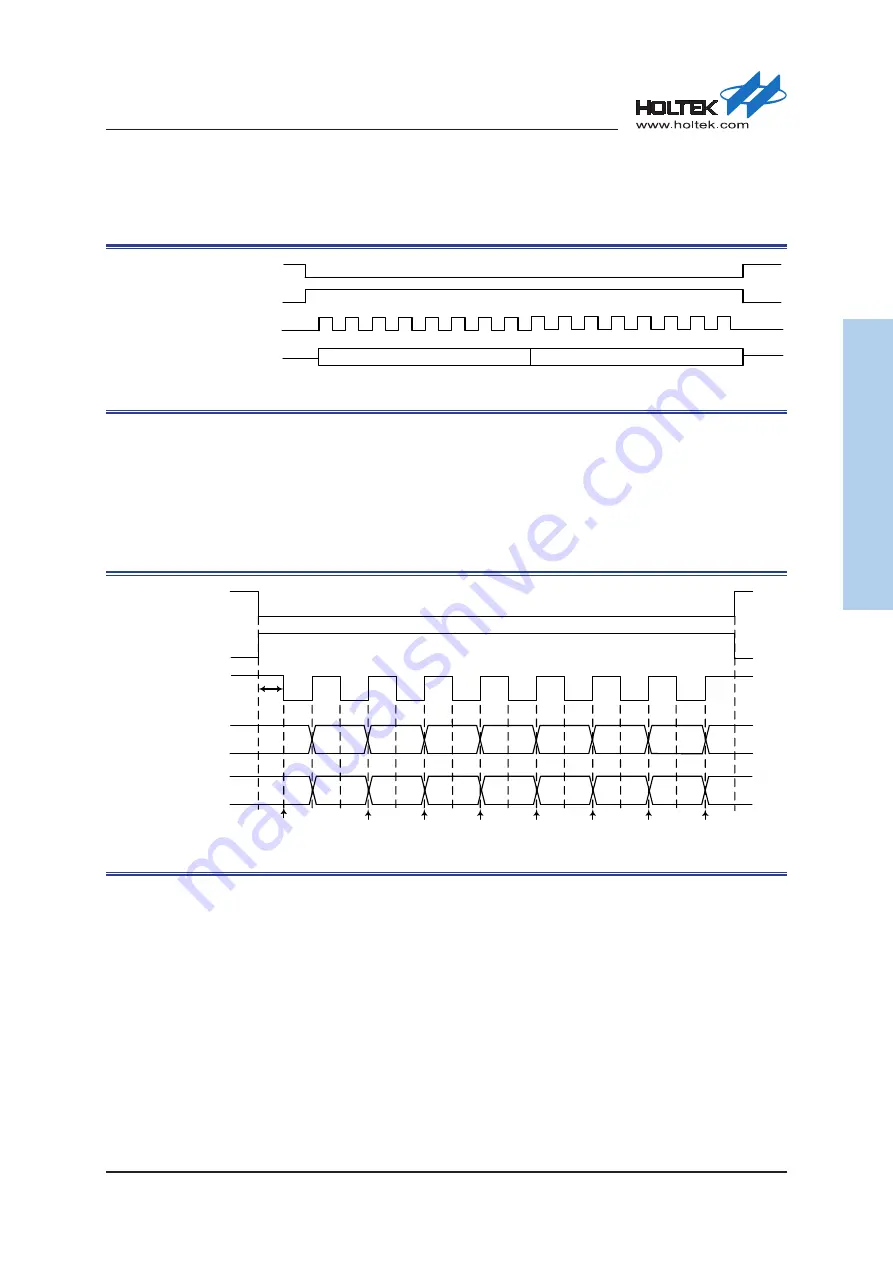
CPOL = 1, CPHA = 0
In this format, the received data is sampled on the SCK line falling edge while the transmitted
data is changed on the SCK line rising edge. In the master mode, the first bit is driven when data
is written into the SPIDR register. In the slave mode, the first bit is driven when the SEL signal
changes to an active level. Figure 157 shows the single byte transfer timing of this format.
SCK
MISO
MOSI
TX[7]
TX[6]
TX[5]
TX[4]
TX[3]
TX[2]
TX[1]
TX[0]
RX[7]
RX[6]
RX[5]
RX[4]
RX[3]
RX[2]
RX[1]
½ SCK
SEL (SELAP=0)
SEL (SELAP=1)
RX[0]
data sampled
Figure 157. SPI Single Byte Transfer Timing Diagram – CPOL = 1, CPHA = 0