______________________________________________
HARRIS
888-9058-001
WARNING: Disconnect and lockout AC primary power prior to servicing
177
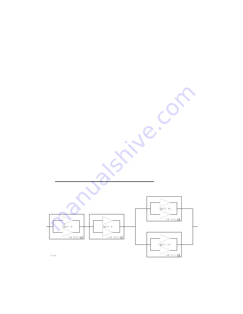
The low band driver module consists of a class A stage, driving a second stage
consisting of two parallel class A amplifier blocks. The bias current per device will be
marked on the hold-down spring clamping bar. This works for analog and digital.
A pi input attenuator (R4, R5, R6 on the Driver RF input assembly) is used to set the
overall gain of each low band driver to 35 dB. The input attenuator also serves to
improve the modules input return loss.
The attenuator output feeds the first amplifier stage, which produces about 24 dB gain.
The output passes to a 2 dB fixed attenuator, used to improve the output match seen by
the first stage.
The RF signal then feeds the 2-way Divider assembly. On this divider assembly there is
in the signal path a microstrip directional coupler (which provides a forward drive
power sample for overdrive protection), a microstrip trombone line section (for phase
adjustment), and a foreshortened Wilkinson 2-way microstrip divider. The dividers two
outputs drive two parallel Class A amplifiers. The outputs are recombined using a
foreshortened Wilkinson microstrip combiner, which passes the signal through a
directional coupler to the module output. The directional coupler provides a reflected
power sample to the modules protection, control and monitor (PCM) system.
On the input and output Driver RF Interconnection assemblies are provided optional
capacitors for response correction. On the input assembly, A5A4, are C1 and C15. On
the driver RF interconnect assembly is C4. A capacitor may be added where needed for
frequency response correction and or input matching. The low band driver output is rated
at 75 Watts average.
8.2.2 Driver Module, High Band (Band II)
Figure 8-3 High Band Driver Module, Simplified Block Diagram
(Refer to the High Band Driver Amplifier Schematic, Tab 1000 in Drawing package)


