


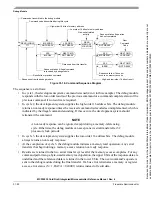


Debug Module
MCF52235 ColdFire® Integrated Microcontroller Reference Manual, Rev. 6
31-22
Freescale Semiconductor
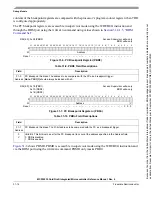
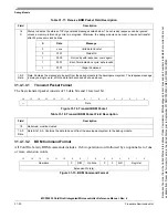
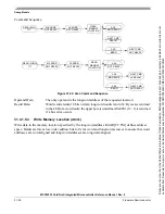
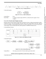
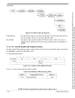
Figure 31-16. Command Sequence Diagram
The sequence is as follows:
•
In cycle 1, the development system command is issued (
READ
in this example). The debug module
responds with the low-order results of the previous command or a command complete status of the
previous command, if no results are required.
•
In cycle 2, the development system supplies the high-order 16 address bits. The debug module
returns a not-ready response unless the received command is decoded as unimplemented, which is
indicated by the illegal command encoding. If this occurs, the development system should
retransmit the command.
NOTE
A not-ready response can be ignored except during a memory-referencing
cycle. Otherwise, the debug module can accept a new serial transfer after 32
processor clock periods.
•
In cycle 3, the development system supplies the low-order 16 address bits. The debug module
always returns a not-ready response.
•
At the completion of cycle 3, the debug module initiates a memory read operation. Any serial
transfers that begin during a memory access return a not-ready response.
•
Results are returned in the two serial transfer cycles after the memory access completes. For any
command performing a byte-sized memory read operation, the upper 8 bits of the response data are
undefined and the referenced data is returned in the lower 8 bits. The next command’s opcode is
sent to the debug module during the final transfer. If a bus error terminates a memory or register
access, error status (S = 1, DATA = 0x0001) returns instead of result data.
XXX
’NOT READY’
READ (LONG)
???
MS ADDR
’NOT READY’
LS ADDR
’NOT READY’
NEXT CMD
’NOT READY’
NEXT CMD
’NOT READY’
NEXT CMD
LS RESULT
Commands transmitted to the debug module
Command code transmitted during this cycle
High-order 16 bits of memory address
Low-order 16 bits of memory address
Non-serial-related
Next
Command
Code
Sequence taken if operation
has not completed
activity
READ
MEMORY
LOCATION
XXX
BERR
XXX
MS RESULT
XXX
’ILLEGAL’
Responses from the debug module
Results from previous command
Sequence taken if illegal command
is received by debug module
Data used from this transfer
Sequence taken if bus error
occurs on memory access
High- and low-order 16 bits of result
Because
of
an
order
from
the
United
States
International
Trade
Commission,
BGA-packaged
product
lines
and
part
numbers
indicated
here
currently
are
not
available
from
Freescale
for
import
or
sale
in
the
United
States
prior
to
September
2010:MCF52234CVM60,
MCF52235CVM60


