
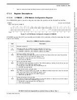


ColdFire Flash Module (CFM)
MCF52235 ColdFire® Integrated Microcontroller Reference Manual, Rev. 6
17-16
Freescale Semiconductor
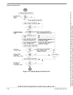
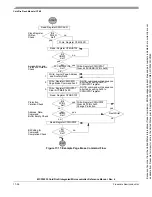
17.4
Functional Description
17.4.1
General
The following modes and operations are described in the following sections:
Section 17.4.2, “Flash Normal Mode
a) Read operation (
Section 17.4.2.1, “Read Operation
”)
b) Write operation (
Section 17.4.2.2, “Write Operation
c) Program, erase, and verify operations (
Section 17.4.2.3, “Program, Erase, and Verify
d) Stop mode (
Section 17.4.3, “Flash Security Operation
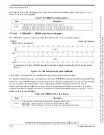
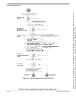
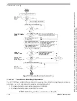
17.4.2
Flash Normal Mode
In flash normal mode, the user can access the CFM registers and the CFM flash memory (see
”).
17.4.2.1
Read Operation
A valid read operation occurs when a transfer request is initiated, the address is equal to an address within
the valid range of the CFM flash memory space and the read/write control indicates a read cycle.
17.4.2.2
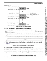
Write Operation
A valid write operation occurs when a transfer request is initiated, the address is equal to an address within
the valid range of the CFM flash memory space and the read/write control indicates a write cycle. The
action taken on a valid flash array write depends on the subsequent user command issued as part of a valid
command write sequence. Only 32-bit write operations are allowed to the flash memory space. Byte and
half-word write operations to the flash memory space results in a cycle termination transfer error.
17.4.2.3
Program, Erase, and Verify Operations
Write and read operations are used for the program, erase, and verify algorithms described in this section.
These algorithms are controlled by the flash memory controller whose timebase, for program and erase
operations, is derived from the internal flash bus clock via a programmable counter. The command register
as well as the associated address and data registers operate as a buffer and a register (2-stage FIFO), so that
a new command along with the necessary data and address can be stored to the buffer while the previous
command remains in progress. This buffering operation provides time optimization when programming
more than one word on a physical row in the flash memory as the high voltage generation can be kept
active in between two programming operations, thereby saving the time overhead needed for setup of the
high voltage charge pumps. Buffer empty as well as command completion are signaled by flags in the
CFMUSTAT register with interrupts generated, if enabled.
The next four sections describe the following:
Because
of
an
order
from
the
United
States
International
Trade
Commission,
BGA-packaged
product
lines
and
part
numbers
indicated
here
currently
are
not
available
from
Freescale
for
import
or
sale
in
the
United
States
prior
to
September
2010:MCF52234CVM60,
MCF52235CVM60


