


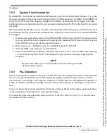


Clock Module
MCF52235 ColdFire® Integrated Microcontroller Reference Manual, Rev. 6
Freescale Semiconductor
7-13
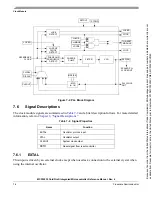
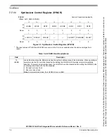
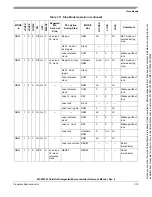
Figure 7-8. Crystal Oscillator Example
7.8.3.1
Phase and Frequency Detector (PFD)
The PFD is a dual-latch phase-frequency detector. It compares the phase and frequency of the reference
and feedback clocks. The reference clock comes from the crystal oscillator or an external clock source.
•
The feedback clock comes from the VCO output divided by the MFD in normal PLL mode.
When the frequency of the feedback clock equals the frequency of the reference clock, the PLL is
frequency-locked. If the falling edge of the feedback clock lags the falling edge of the reference clock, the
PFD pulses the UP signal. If the falling edge of the feedback clock leads the falling edge of the reference
clock, the PFD pulses the DOWN signal. The width of these pulses relative to the reference clock depends
on how much the two clocks lead or lag each other. After phase lock is achieved, the PFD continues to
pulse the UP and DOWN signals for very short durations during each reference clock cycle. These short
pulses continually update the PLL and prevent the frequency drift phenomenon known as dead-banding.
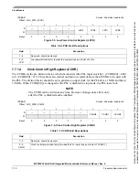
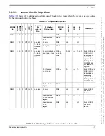
7.8.3.2
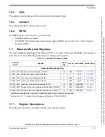
Charge Pump/Loop Filter
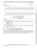
In normal mode the current magnitude of the charge pump varies with the MFD as shown in
The UP and DOWN signals from the PFD control whether the charge pump applies or removes charge,
respectively, from the loop filter. The filter is integrated on the chip.
7.8.3.3
Voltage Control Output (VCO)
The voltage across the loop filter controls the frequency of the VCO output. The frequency-to-voltage
relationship (VCO gain) is positive, and the output frequency is four times the target system frequency.
Table 7-9. Charge Pump Current and MFD in Normal Mode Operation
Charge Pump Current
MFD
1x
0
≤
MFD < 2
2x
2
≤
MFD < 6
4x
6
≤
MFD
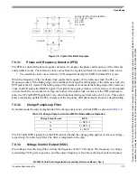
V
SSPLL
V
SSPLL
EXTAL
XTAL
RS
RF
C1
C2
ON-CHIP
25-MHz CRYSTAL CONFIGURATION
C1 = 15 pF, C2 = 39pF
RF = 1 M
Ω
RS = 470
Ω
R1
R1 = 10 M
Ω
Because
of
an
order
from
the
United
States
International
Trade
Commission,
BGA-packaged
product
lines
and
part
numbers
indicated
here
currently
are
not
available
from
Freescale
for
import
or
sale
in
the
United
States
prior
to
September
2010:MCF52234CVM60,
MCF52235CVM60


