


Analog-to-Digital Converter (ADC)
MCF52235 ColdFire® Integrated Microcontroller Reference Manual, Rev. 6
28-23
Freescale Semiconductor
Optional interrupts can be generated at the end of a scan sequence. Interrupts are available simply to
indicate the scan ended, that a sample was out of range, or at several different zero crossing conditions.
Out-of-range is determined by the high and low limit registers.
To understand the operation of the ADC, it is important to understand the features and limitations of each
of the functional parts.
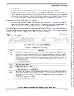
28.5.1
Input MUX Function
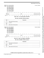
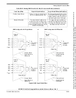
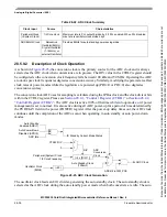
The input MUX function is shown in
The channel select and single ended vs. differential
switches are indirectly controlled based on settings within the LIST1, LIST2, and SDIS registers, and the
CHNCFG field of the CTRL1 register.
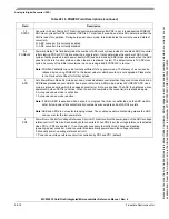
1. MUXing for Sequential mode, single-ended conversions—During each conversion cycle (sample),
any one input of the two muxes can be directed to any ADRSLT
n
register.
2. MUXing for sequential mode, differential conversions—During any conversion cycle (sample),
either member of a differential pair may be referenced as a SAMPLE, resulting in a differential
measurement on that pair being stored in the corresponding ADRSLT
n
register.
3. MUXing for parallel mode, single-ended conversions—During any conversion cycle (sample), any
of AN0-AN3 can be directed to ADRSLT0-3 and any of AN4-AN7 can be directed to ADRSLT4-7.
4. MUXing for parallel mode, differential conversions—During any conversion cycle (sample),
either member of differential pair AN0/1 or either member of differential pair AN2/3 can be
referenced as a SAMPLE, resulting in a differential measurement of that pair being stored in one
of the ADRSLT0-3 registers. Likewise, either member of differential pair AN4/5 or either member
of differential pair AN6/7 can be referenced as a SAMPLE, resulting in a differential measurement
of that pair being stored in one of the ADRSLT4-7 registers.
Details of switch operation is shown in
Internally, all measurements are performed
differentially. During single ended measurements, V
REFL
is used as the negative (-) input voltage, while
the selected analog input is used as the positive (
+
) input.
Table 28-20. Analog MUX Controls for Each Conversion Mode
Conversion Mode
Channel Select Switches
Single Ended Differential Switches
Sequential, Single Ended
The two 1-of-4 select muxes can be
set for the appropriate input line.
The lower switch selects V
REFL
for the
V- input of the A/D. The upper switch is
always closed so that any of the four
inputs can get to the V+ A/D input.
Sequential, Differential
The channel select switches are
turned on in pairs, providing a dual
1-of-2 select function, such that either
of the two differential channels can be
routed to the A/D input.
The upper switch is open and the
bottom switch selects the differential
channel for the V- input of the A/D.
Because
of
an
order
from
the
United
States
International
Trade
Commission,
BGA-packaged
product
lines
and
part
numbers
indicated
here
currently
are
not
available
from
Freescale
for
import
or
sale
in
the
United
States
prior
to
September
2010:MCF52234CVM60,
MCF52235CVM60


