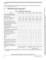
Freescale Semiconductor MCF52230 ColdFire Скачать руководство пользователя страница 1

MCF52235 ColdFire

®

 Integrated

Microcontroller Reference Manual

Devices Supported:

MCF52230
MCF52231
MCF52232
MCF52233
MCF52234
MCF52235
MCF52236

Document Number:

MCF52235RM

Rev. 6

07/2010

Because 

of 

an 

order 

from 

the 

United 

States 

International 

Trade 

Commission, 

BGA-packaged 

product 

lines 

and 

part 

numbers 

indicated 

here 

currently 

are 

not 

available 

from 

Freescale 

for 

import 

or 

sale 

in 

the 

United 

States 

prior 

to 

September 

2010:MCF52234CVM60, 

MCF52235CVM60

Содержание MCF52230 ColdFire

Страница 1: ...CF52235 MCF52236 Document Number MCF52235RM Rev 6 07 2010 Because of an order from the United States International Trade Commission BGA packaged product lines and part numbers indicated here currently...

Страница 2: ...ing without limitation consequential or incidental damages Typical parameters that may be provided in Freescale Semiconductor data sheets and or specifications can and do vary in different application...

Страница 3: ...le Signals 2 12 2 11 DMA Timer Signals 2 12 2 12 ADC Signals 2 12 2 13 General Purpose Timer Signals 2 13 2 14 Pulse Width Modulator Signals 2 13 2 15 Debug Support Signals 2 13 2 16 EzPort Signal Des...

Страница 4: ...7 6 Signal Descriptions 7 4 7 7 Memory Map and Registers 7 5 7 8 Functional Description 7 11 Chapter 8 Real Time Clock 8 1 Introduction 8 1 8 2 Memory Map Register Definition 8 2 8 3 Functional Descr...

Страница 5: ...gister Definition 13 2 13 5 Register Descriptions 13 3 13 6 Internal Bus Arbitration 13 9 13 7 System Access Control Unit SACU 13 12 Chapter 14 General Purpose I O Module 14 1 Introduction 14 1 14 2 O...

Страница 6: ...iptors 18 47 Chapter 19 Ethernet Physical Transceiver EPHY 19 1 Introduction 19 1 19 2 External Signal Descriptions 19 3 19 3 Memory Map and Register Descriptions 19 5 19 4 Functional Description 19 2...

Страница 7: ...8 24 4 Initialization Application Information 24 9 Chapter 25 Queued Serial Peripheral Interface QSPI 25 1 Introduction 25 1 25 2 External Signal Description 25 2 25 3 Memory Map Register Definition...

Страница 8: ...Map Register Definition 30 5 30 4 Initialization Application Information 30 28 Chapter 31 Debug Module 31 1 Introduction 31 1 31 2 Signal Descriptions 31 2 31 3 Memory Map Register Definition 31 3 31...

Страница 9: ...iconductor ix Because of an order from the United States International Trade Commission BGA packaged product lines and part numbers indicated here currently are not available from Freescale for import...

Страница 10: ...ules include the following V2 ColdFire core with enhanced multiply accumulate unit EMAC Cryptographic Acceleration Unit CAU Up to 32 Kbytes of internal SRAM Up to 256 Kbytes of on chip flash memory Fa...

Страница 11: ...2 0B Module Fast Ethernet Controller FEC with on chip interface EPHY Four channel Direct Memory Access DMA Software Watchdog Timer WDT Programmable Interrupt Timer 2 2 2 2 2 2 2 Four Channel General P...

Страница 12: ...IM 2 DTIM 3 V2 ColdFire CPU IFP OEP EMAC 4 CH DMA MUX JTAG TAP To From PADI 32 Kbytes SRAM 4K 16 4 256 Kbytes Flash 32K 16 4 PORTS GPIO CIM RSTIN RSTOUT SDA SCL UTXDn URXDn URTSn DTINn DTOUTn CANRX JT...

Страница 13: ...31CAL60 MCF52231 Microcontroller FlexCAN 60 128 32 112 LQFP 40 to 85 MCF52232CAF50 MCF52232 Microcontroller 50 128 32 80 LQFP 40 to 85 MCF52232AF50 MCF52232 Microcontroller 50 128 32 80 LQFP 0 to 70 M...

Страница 14: ...C 10 100 BaseT TX capability half duplex or full duplex On chip transmit and receive FIFOs Built in dedicated DMA controller Memory based flexible descriptor rings On chip Ethernet Transceiver EPHY Di...

Страница 15: ...or two UARTs Transmit and receive FIFO buffers I2C module Interchip bus interface for EEPROMs LCD controllers A D converters and keypads Fully compatible with industry standard I2 C bus Master and sla...

Страница 16: ...tes as eight channels with 8 bit resolution or four channels with 16 bit resolution Programmable period and duty cycle Programmable enable disable for each channel Software selectable polarity for eac...

Страница 17: ...data capability along with support for 16 byte 4 x 32 bit burst transfers Source destination address pointers that can increment or remain constant 24 bit byte transfer counter per channel Auto alignm...

Страница 18: ...rocessor at a minimal hardware cost 1 4 2 Integrated Debug Module The ColdFire processor core debug interface is provided to support system debugging in conjunction with low cost debug and emulator de...

Страница 19: ...g the boundary scan register to a single bit Disable the output drive to pins during circuit board testing Drive output pins to stable levels 1 4 4 On Chip Memories 1 4 4 1 SRAM The dual ported SRAM m...

Страница 20: ...e cost 1 4 6 Power Management The MCF52235 incorporates several low power modes of operation which are entered under program control and exited by several external trigger events An integrated power o...

Страница 21: ...pendent DMA transfer capable 32 bit timers DTIM0 DTIM1 DTIM2 and DTIM3 on the each device Each module incorporates a 32 bit timer with a separate register set for configuration and control The timers...

Страница 22: ...untdown 1 4 17 Phase Locked Loop PLL The clock module contains a crystal oscillator 8 MHz on chip relaxation oscillator OCO phase locked loop PLL reduced frequency divider RFD low power divider status...

Страница 23: ...pability in addition to their primary functions and are grouped into 8 bit ports Some ports do not utilize all 8 bits Each port has registers that configure monitor and control the port pins 1 4 22 1...

Страница 24: ...troller FIFO Memory 0x4000_1800 1M 6K Reserved 0x4010_0000 64K Ports 0x4011_0000 64K CIM_IBO 0x4012_0000 64K Clocks PLLMRBI 0x4013_0000 64K Edge Port 0 0x4014_0000 64K Edge Port 1 0x4015_0000 64K Prog...

Страница 25: ...ory for IPS reads and writes 0x4408_0000 1G 64M 256K Reserved 0x8000_0000 2G Reserved Table 1 3 System Memory Map continued Base Address Hex Size Use Because of an order from the United States Interna...

Страница 26: ...d confusion when dealing with a mixture of active low and active high signals The term asserted indicates that a signal is active independent of the voltage level The term negated indicates that a sig...

Страница 27: ...16 4 PORTS GPIO CIM RSTIN RSTOUT SDA SCL UTXDn URXDn URTSn DTINn DTOUTn CANRX JTAG_EN ADC AN 7 0 VRH VRL PLL CLKGEN Edge Port 2 FlexCAN EXTAL XTAL CLKOUT RNGA PIT1 GPT PWM To From Interrupt Controlle...

Страница 28: ...AN 1 Low A9 91 67 AN0 PAN 0 Low C8 92 68 SYNCA CANTX4 FEC_MDIO PAS 3 PDSR 39 K1 28 20 SYNCB CANRX4 FEC_MDC PAS 2 PDSR 39 J1 27 19 VDDA N A N A A8 93 69 VSSA N A N A A7 96 72 VRH N A N A B8 94 70 VRL N...

Страница 29: ...RX5 N A F10 75 55 PHY_VDDTX5 N A G10 69 49 PHY_VSSA N A G8 67 47 PHY_VSSRX N A F9 76 56 PHY_VSSTX N A G9 72 52 I2C SCL CANTX4 UTXD2 PAS 0 PDSR 0 Pull Up6 A3 111 79 SDA CANRX4 URXD2 PAS 1 PDSR 0 Pull U...

Страница 30: ...ull Up6 K8 54 IRQ1 SYNCA PWM1 PNQ 1 High Pull Up6 J8 55 39 JTAG BDM JTAG_EN N A N A Pull Down G4 18 12 TCLK PSTCLK CLKOUT High Pull Up7 A1 1 1 TDI DSI N A N A Pull Up7 C3 4 4 TDO DSO High N A C2 5 5 T...

Страница 31: ...PWM7 PTA 3 PDSR 23 Pull Up10 B4 107 75 GPT2 FEC_TXD 2 PWM5 PTA 2 PDSR 22 Pull Up10 C4 108 76 GPT1 FEC_TXD 1 PWM3 PTA 1 PDSR 21 Pull Up10 D4 109 77 GPT0 FEC_TXER PWM1 PTA 0 PDSR 20 Pull Up10 B3 110 78...

Страница 32: ...hapter 14 General Purpose I O Module All programmable signals default to 2mA drive in normal single chip mode 2 All signals have a pull up in GPIO mode 3 The use of an external PHY limits ADC interrup...

Страница 33: ...PIO function Primary Function has pull up control within the GPT module 11 This list for power and ground does not include those dedicated power ground pins included elsewhere e g in the Ethernet PHY...

Страница 34: ...Crystal oscillator or external clock input I Crystal XTAL Crystal oscillator output O Clock Out CLKOUT This output signal reflects the internal system clock O Table 2 4 Mode Selection Signals Signal...

Страница 35: ...onous Serial Data Input QSPI_DIN Provides the serial data to the QSPI and can be programmed to be sampled on the rising or falling edge of QSPI_CLK I QSPI Serial Clock QSPI_CLK Provides the serial clo...

Страница 36: ...tance must be kept to less than 10 pF 50 pF causes instability No high speed signals can be permitted in the region of RBIAS I Activity LED ACT_LED Indicates when the EPHY is transmitting or receiving...

Страница 37: ...pped for power down mode any transition on this pin restarts it I Clear to Send UCTSn Indicate to the UART modules that they can begin data transmission I Request to Send URTSn Automatic request to se...

Страница 38: ...e machine TMS is sampled on the rising edge of TCLK I Test Data Input TDI Serial input for test instructions and data TDI is sampled on the rising edge of TCLK I Test Data Output TDO Serial output for...

Страница 39: ...g without disabling triggers Non quiescent operation can be reenabled by clearing CSR PCD although the external development systems must resynchronize with the PST and DDATA outputs PSTCLK starts cloc...

Страница 40: ...id connecting power supply voltage directly to pins in Figure 2 which show only capacitor connections as doing so could damage the device severely Table 2 16 Power and Ground Pins Signal Name Abbrevia...

Страница 41: ...SX2 VDD2 VSS2 VDD1 VSS1 0 1 F 10 H 10 F 10V Tantalum 0 1 F 0 1 F 0 1 F 0 22 F 0 22 F 3 3V 48 49 PHY_V DDA PHY_V DDTX 0 22 F 55 46 PHY_V DDRX PHY_RBIAS 0 22 F 0 22 F 12 4K 1 0 1 F Pin numbering is show...

Страница 42: ...dFire Core Pipelines The instruction fetch pipeline IFP is a two stage pipeline for prefetching instructions The prefetched instruction stream is then gated into the two stage operand execution pipeli...

Страница 43: ...hrough both OEP stages once For memory to register and read modify write memory operations an instruction is effectively staged through the OEP twice the first time to calculate the effective address...

Страница 44: ...isters Load 0x080 Store 0x180 Data Register 0 D0 32 R W 0xCF2_6 No 3 2 1 3 4 Load 0x081 Store 0x181 Data Register 1 D1 32 R W 0x No 3 2 1 3 4 Load 0x082 7 Store 0x182 7 Data Register 2 7 D2 D7 32 R W...

Страница 45: ...16 R W 0x27 No 3 2 7 3 7 0xC04 Flash Base Address Register FLASHBAR 32 R W 0x0000_0000 Yes 3 2 8 3 8 0xC05 RAM Base Address Register RAMBAR 32 R W See Section Yes 3 2 8 3 8 1 The values listed in this...

Страница 46: ...A7 and OTHER_A7 to the two program visible definitions SSP and USP To support dual stack pointers the following two supervisor instructions are included in the ColdFire instruction set architecture to...

Страница 47: ...6 5 4 3 2 1 0 R 0 0 0 X N Z V C W Reset 0 0 0 Figure 3 5 Condition Code Register CCR Table 3 2 CCR Field Descriptions Field Description 7 5 Reserved must be cleared 4 X Extend condition code bit Set...

Страница 48: ...tware can access the entire SR In user mode only the lower 8 bits CCR are accessible The control bits indicate the following states for the processor trace mode T bit supervisor or user mode S bit and...

Страница 49: ...software can set it during execution of the RTE or move to SR instructions 11 Reserved must be cleared 10 8 I Interrupt level mask Defines current interrupt level Interrupt requests are inhibited for...

Страница 50: ...AG stage and the resulting prefetch address gated onto the core bus if there are no pending operand memory accesses assigned a higher priority After the prefetch address is driven onto the core bus th...

Страница 51: ...y mem x For simple register to register instructions the first stage of the OEP performs the instruction decode and fetching of the required register operands OC from the dual ported register file whi...

Страница 52: ...32 bit load instruction move l mem y Rx is optimized to support a two cycle execution time The following example in Figure 3 12 shows an effective address of the form ea y d16 Ay i e a 16 bit signed...

Страница 53: ...lacement added to a base register Ax For read modify write instructions the pipeline effectively combines an embedded load with a store operation for a three cycle execution time Operand Execution Pip...

Страница 54: ...and the various instruction operations are shown progressing down the operand execution pipeline Operand Execution Pipeline DSOC AGEX Opword Extension 1 Extension 2 Core Bus Read Data Core Bus Addres...

Страница 55: ...that could be improved by the creation of additional instructions The original ISA definition minimized support for instructions referencing byte and word sized operands Full support for the move byte...

Страница 56: ...t request level Table 3 4 Instruction Enhancements over Revision ISA_A Instruction Description BITREV The contents of the destination data register are bit reversed new Dn 31 equals old Dn 0 new Dn 30...

Страница 57: ...r the first opcode of the handler has initiated exception processing terminates and normal instruction processing continues in the handler The table contains 256 exception vectors the first 64 are def...

Страница 58: ...r 7 by the processor indicating a two longword frame format See Table 3 6 There is a 4 bit fault status field FS 3 0 at the top of the system stack This field is defined for access and address errors...

Страница 59: ...auto addressing modes for example An An have already been performed so the programming model contains the updated An value In addition if an access error occurs during a MOVEM instruction loading fro...

Страница 60: ...three instruction sizes 16 32 or 48 bits The first instruction word is known as the operation word or opword while the optional words are known as extension word 1 and extension word 2 The opword is...

Страница 61: ...ode instruction but if the debug module s CSR UHE is set then this instruction can be also be executed in user mode for debugging purposes 3 3 4 6 Trace Exception To aid in program development all Col...

Страница 62: ...F opcode 3 3 4 9 Debug Interrupt See Chapter 31 Debug Module for a detailed explanation of this exception which is generated in response to a hardware breakpoint register trigger The processor does no...

Страница 63: ...or causes a reset exception The reset exception has the highest priority of any exception it provides for system initialization and recovery from catastrophic failure Reset also aborts any processing...

Страница 64: ...he value used for this device 0011 V3 ColdFire core 0100 V4 ColdFire core 0101 V5 ColdFire core Else Reserved for future use 19 16 REV Processor revision number The default is 0b0000 15 MAC MAC presen...

Страница 65: ...Access User read only BDM read only 31 30 29 28 27 26 25 24 23 22 21 20 19 18 17 16 R CLSZ CCAS CCSZ FLASHSZ 0 0 0 W 15 14 13 12 11 10 9 8 7 6 5 4 3 2 1 0 R MBSZ UCAS 0 0 0 0 SRAMSZ 0 0 0 W Figure 3 1...

Страница 66: ...e cache 0100 4 KB configurable cache 0101 8 KB configurable cache 0110 16 KB configurable cache 0111 32 KB configurable cache Else Reserved 23 19 FLASHSZ Flash bank size 00000 01110 No flash 10000 64...

Страница 67: ...cycles The MOVEM instruction uses a different set of resources and this stall does not apply 3 The OEP completes all memory accesses without any stall conditions caused by the memory itself Thus the...

Страница 68: ...1 3 1 1 3 1 1 d16 PC 3 1 0 3 1 1 3 1 1 3 1 1 3 1 1 d8 PC Xi SF 4 1 0 4 1 1 4 1 1 4 1 1 xxx 1 0 0 3 0 1 3 0 1 3 0 1 Table 3 13 MOVE Long Execution Times Source Destination Rx Ax Ax Ax d16 Ax d8 Ax Xi...

Страница 69: ...1 0 3 1 0 3 1 0 4 1 0 3 1 0 1 0 0 TST W ea 1 0 0 3 1 0 3 1 0 3 1 0 3 1 0 4 1 0 3 1 0 1 0 0 TST L ea 1 0 0 2 1 0 2 1 0 2 1 0 2 1 0 3 1 0 2 1 0 1 0 0 Table 3 15 Two Operand Instruction Execution Times O...

Страница 70: ...0 38 1 0 38 1 0 EOR L Dy ea 1 0 0 3 1 1 3 1 1 3 1 1 3 1 1 4 1 1 3 1 1 EORI L imm Dx 1 0 0 LEA ea Ax 1 0 0 1 0 0 2 0 0 1 0 0 LSL L ea Dx 1 0 0 1 0 0 LSR L ea Dx 1 0 0 1 0 0 MOVEQ L imm Dx 1 0 0 OR L e...

Страница 71: ...0 STLDSR imm 5 0 1 STOP imm 3 0 0 3 TRAP imm 15 1 2 TPF 1 0 0 TPF W 1 0 0 TPF L 1 0 0 UNLK Ax 2 1 0 WDDATA ea 3 1 0 3 1 0 3 1 0 3 1 0 4 1 0 3 1 0 WDEBUG ea 5 2 0 5 2 0 1The n is the number of register...

Страница 72: ...0 2 2 Storing an accumulator requires one additional processor clock cycle when saturation is enabled or fractional rounding is performed MACSR 7 4 equals 1 11 11 MOVE L MACSR ea x 1 0 0 MOVE L Rmask...

Страница 73: ...C pipeline is exposed and the execution time is four cycles 3 3 5 7 Branch Instruction Execution Times Table 3 18 General Branch Instruction Execution Times Opcode EA Effective Address Rn An An An d16...

Страница 74: ...lly pipelined 32 32 multiply array and four 48 bit accumulators The first ColdFire MAC supported signed and unsigned integer operands and was optimized for 16x16 operations such as those found in appl...

Страница 75: ...his functionality is common in many signal processing applications The ColdFire core architecture is also modified to allow an operand to be fetched in parallel with a multiply increasing overall perf...

Страница 76: ...ed 4 2 3 4 7 0x807 MAC Accumulator 0 1 Extension Bytes ACCext01 32 R W Undefined 4 2 4 4 7 0x808 MAC Accumulator 2 3 Extension Bytes ACCext23 32 R W Undefined 4 2 4 4 7 0x809 MAC Accumulator 1 ACC1 32...

Страница 77: ...value Accumulator is moved to a general purpose register as a 32 bit value 1 The accumulator is rounded to a 16 bit value using the round to nearest even method when moved to a general purpose regist...

Страница 78: ...th of the EMAC V is set only if a product overflow occurs or the accumulation overflows the 48 bit structure V is evaluated on each MAC or MSAC operation and uses the appropriate PAVn flag in the next...

Страница 79: ...d16 An oa An se_d16 0xFFFF0x MASK Here oa is the calculated operand address and se_d16 is a sign extended 16 bit displacement For auto addressing modes of post increment and pre decrement the updated...

Страница 80: ...BDM read write 31 30 29 28 27 26 25 24 23 22 21 20 19 18 17 16 15 14 13 12 11 10 9 8 7 6 5 4 3 2 1 0 R Accumulator W Reset Table 4 5 ACC0 3 Field Descriptions Field Description 31 0 Accumulator Store...

Страница 81: ...s optimized for single cycle pipelined 32 32 multiplications For word and longword sized integer input operands the low order 40 bits of the product are formed and used with the destination accumulato...

Страница 82: ...Accumulator 47 0 ACCextn 15 0 ACCn 31 0 if MACSR 6 5 01 or 11 signed fractional mode Complete Accumulator 47 0 ACCextn 15 8 ACCn 31 0 ACCextn 7 0 if MACSR 6 5 10 unsigned integer mode Complete Accumu...

Страница 83: ...operand simultaneously from memory into a register and execute a MAC instruction makes some DSP operations such as filtering and convolution more manageable The programming model includes a mask regis...

Страница 84: ...t rounding modes must be disabled during the save restore process so the exact bit wise contents of the EMAC registers are accessed Consider the memory structure containing the EMAC programming model...

Страница 85: ...esult Multiply Accumulate mac Ry RxSF ACCx msac Ry RxSF ACCx Multiplies two operands and adds subtracts the product to from an accumulator Multiply Accumulate with Load mac Ry Rx ea y Rw ACCx msac Ry...

Страница 86: ...s the store accumulator instruction for three cycles the EMAC pipleline depth minus 1 The minus 1 factor is needed because the OEP and EMAC pipelines overlap by a cycle the AGEX stage As the store acc...

Страница 87: ...ectively The largest positive word is 0x7FFF or 1 2 15 the most positive longword is 0x7FFF_FFFF or 1 2 31 4 3 5 MAC Opcodes MAC opcodes are described in the ColdFire Programmer s Reference Manual Rem...

Страница 88: ...vering the three basic operating modes with signed integers unsigned integers and signed fractionals Throughout this example a comma separated list in curly brackets indicates a concatenation operatio...

Страница 89: ...SR PAVn 1 MACSR V 1 if MACSR OMC 1 then accumulation overflow saturationMode enabled if result 47 1 then result 47 0 0x0000_7fff_ffff else result 47 0 0xffff_8000_0000 transfer the result to the accum...

Страница 90: ...roduct 71 24 else result 47 0 ACCx 47 0 product 71 24 check for accumulation overflow if accumulationOverflow 1 then MACSR PAVn 1 MACSR V 1 if MACSR OMC 1 then accumulation overflow saturationMode ena...

Страница 91: ...te scale product before combining with accumulator switch SF 2 bit scale factor case 0 no scaling specified break case 1 SF 1 product 40 0 product 39 0 0 break case 2 reserved encoding break case 3 SF...

Страница 92: ...0 MACSR V MACSR PAVn MACSR N ACCx 47 if ACCx 47 0 0x0000_0000_0000 then MACSR Z 1 else MACSR Z 0 if ACCx 47 32 0x0000 then MACSR EV 0 else MACSR EV 1 break Because of an order from the United States I...

Страница 93: ...lock Diagram Figure 5 1 shows a simplified block diagram of the CAU Figure 5 1 Top Level CAU Block Diagram 5 1 2 Overview The CAU supports acceleration of the following algorithms DES 3DES AES MD5 ALU...

Страница 94: ...rs It is tightly coupled to the ColdFire core and there is no local memory or external interface 5 1 3 Features The CAU includes these distinctive features Supports DES 3DES AES MD5 SHA 1 algorithms S...

Страница 95: ...he value on this device 0x2 Second version added support for SHA 256 algorithm 27 2 Reserved must be cleared 1 DPE DES parity error 0 No error detected 1 DES key parity error detected 0 IC Illegal com...

Страница 96: ...is cp0ld l ea CMD coprocessor load cp0st l ea CMD coprocessor store The ea field specifies the source operand operand1 for load instructions and destination result for store instructions The basic Col...

Страница 97: ...cp0ld MVRA Move Reg to Acc 0x08 CAx CAx CAA cp0ld MVAR Move Acc to Reg 0x09 CAx CAA CAx cp0ld AESS AES Sub Bytes 0x0A CAx SubBytes CAx CAx cp0ld AESIS AES Inv Sub Bytes 0x0B CAx InvSubBytes CAx CAx c...

Страница 98: ...he LDR command loads CAx with the source data specified by ea 5 3 3 3 Store Register STR cp0st l ea STR CAx The STR command stores the value from CAx to the destination specified by ea 5 3 3 4 Add to...

Страница 99: ...e substitution operation on CAx and stores the result back to CAx 5 3 3 12 AES Inverse Substitution AESIS cp0ld l AESIS CAx The AESIS command performs the AES inverse byte substitution operation on CA...

Страница 100: ...tial permutation performs on CA2 and CA3 after the round operation The round operation uses the source values from registers CA0 and CA1 for the key addition operation The KSx field specifies the shif...

Страница 101: ...t to the value in CAA and stores the result in CAA The specific hash function performed is based on the HFx field as defined in Table 5 10 5 3 3 20 Secure Hash Shift SHS cp0ld l SHS The SHS command do...

Страница 102: ...er A0 is pointing to the key schedule cp0ld l AESS CA0 sub bytes w0 cp0ld l AESS CA1 sub bytes w1 cp0ld l AESS CA2 sub bytes w2 cp0ld l AESS CA3 sub bytes w3 cp0ld l AESR shift rows cp0ld l a0 AESC CA...

Страница 103: ...left 2 bits set KSR1 0x02 key schedule right 1 bit set KSR2 0x03 key schedule right 2 bits DESK Field set DC 0x01 decrypt key schedule set CP 0x02 check parity HASH Functions Codes set HFF 0x0 MD5 F C...

Страница 104: ...plication the attack is based on the linearity of the internal shift registers In light of this it is highly recommended to use the random data produced by this module as an input seed to a NIST appro...

Страница 105: ...read write 31 30 29 28 27 26 25 24 23 22 21 20 19 18 17 16 15 14 13 12 11 10 9 8 7 6 5 4 3 2 1 0 R 0 0 0 0 0 0 0 0 0 0 0 0 0 0 0 0 0 0 0 0 0 0 0 0 0 0 0 SLM 0 IM HA GO W CI Reset 0 0 0 0 0 0 0 0 0 0...

Страница 106: ...3 16 OFS Output FIFO size Indicates size of the output FIFO 1 word and maximum possible value of RNGR OFL 15 8 OFL Output FIFO level Indicates current number of random words in the output FIFO Determi...

Страница 107: ...he FIFO every 256 clock cycles as long as RNGOUT is not full It is very important to poll RNGSR OFL to make sure random values are present before reading from RNGOUT 1 LRS Last read status Reflects st...

Страница 108: ...r all addressable registers and control state machines for the RNG This block is responsible for communication with the peripheral interface and the FIFO interface The block also controls the core eng...

Страница 109: ...l 3 Write to the RNG control register and set the interrupt mask high assurance and GO bits 4 Poll RNGSR OFL to check for random data in RNGOUT 5 Read available random data from RNGOUT 6 Repeat steps...

Страница 110: ...module contains the following Crystal amplifier and oscillator OSC Phase locked loop PLL Reduced frequency divider RFD Status and control registers Control logic 7 2 Features Features of the clock mod...

Страница 111: ...uickly enabling the system clocks during stop recovery This eliminates the wakeup recovery time but at the risk of sending a potentially unstable clock to the system To prevent a non locked PLL freque...

Страница 112: ...t Controllers PPMRL 16 13 DMA Timers PPMRL 10 QSPI PPMRL 9 I2 C PPMRL 7 5 UARTs PPMRL 4 DMA ColdFire V2 Core BDM PITs DISCLK PPMRL 1 2 System Clock fsys Pre Divider CCHR MHz OSCILLATOR XTAL PPMRL 21 F...

Страница 113: ...Signal Properties Name Function EXTAL Oscillator or clock input XTAL Oscillator output CLKOUT System clock output RSTO Reset signal from reset controller STPMD RSTOUT MFD 4 18 LOCKS LOCK LOCS TO RESET...

Страница 114: ...a register and undefined register bits are reserved for expansion Register Width bits Access Reset Value Section Page Supervisor Mode Access Only 0x0012_0000 Synthesizer Control Register SYNCR 16 R W...

Страница 115: ...d Descriptions Field Description 15 LOLRE Loss of lock reset enable Determines how the system handles a loss of lock indication When operating in normal mode the PLL must be locked before setting the...

Страница 116: ...he PLL 1 Bypass the PLL 2 Update RFD 3 Select the PLL clock again The LPD Low Power Divider register can also be used to change system clock frequency 7 LOCEN Enables the loss of clock function LOCEN...

Страница 117: ...er is ensured 0 PLLreference clock input clock drives the system clock 1 PLL output clock drives the system clock provided the PLL is enabled 1 PLLMODE Determines the operating mode of the PLL This bi...

Страница 118: ...PLL loses lock when a frequency deviation of greater than approximately 1 5 occurs Reading the LOCK flag at the same time that the PLL loses lock or acquires lock does not return the current conditio...

Страница 119: ...CCHR IPSBAR Offset 0x12_0007 LPCR Access Supervisor read write 7 6 5 4 3 2 1 0 R LPD3 LPD2 LPD1 LPD0 W Reset 0 0 0 0 0 0 0 0 Figure 7 5 Low Power Control Register LPCR Table 7 6 LPCR Field Description...

Страница 120: ...gh this mode also supports an external clock source After out of reset it is not possible to change the input clock source although it is possible to enable the PLL and switch between the PLL clock an...

Страница 121: ...om step 1 to the SYNCR 4 Monitor the LOCK flag in SYNSR When the PLL achieves lock write the RFD value from step 1 to the RFD field of the SYNCR This changes the system clocks frequency to the require...

Страница 122: ...signals for very short durations during each reference clock cycle These short pulses continually update the PLL and prevent the frequency drift phenomenon known as dead banding 7 8 3 2 Charge Pump Lo...

Страница 123: ...ed by the PLL feedback When the reference counter has counted N cycles its count is compared to that of the feedback counter If the feedback counter has also counted N cycles the process is repeated f...

Страница 124: ...in the SYNCR is set a loss of lock condition asserts reset Reset reinitializes the LOCK and LOCKS flags Therefore software must read the LOL bit in the reset status register RSR to determine if a loss...

Страница 125: ...erence fails the PLL goes out of lock and into self clocked mode SCM The PLL remains in SCM until the next reset When the PLL is operating in SCM the system frequency depends on the value in the RFD f...

Страница 126: ...reference clock Regain clocks but don t regain lock SCM unstable NRM 0 LK 0 1 1 LC Block LOCS and LOCKS until clock and lock respectively regain enter SCM regardless of LOCEN bit until reference regai...

Страница 127: ...k Unstable NRM 0 0 1 LC Lose clock regain with lock NRM 0 1 LC NRM X X 1 Off X X Lose lock f b clock reference clock RESET RESET Reset immediately NRM 0 0 1 On On X NRM LK 1 LC Lose lock or clock RESE...

Страница 128: ...lock Lose lock Stuck Lose lock regain NRM 0 1 LC NRM 1 0 0 On On 1 NRM LK 1 LC Lose reference clock SCM 0 0 1 Wakeup without lock Lose f b clock REF 0 X 1 Wakeup without lock Lose lock Unstable NRM 0...

Страница 129: ...erence clock Stuck SCM 1 0 0 Off X 0 PLL disabled Regain SCM SCM 0 0 1 Wakeup without lock SCM 1 0 0 Off X 1 PLL disabled Regain SCM SCM 0 0 1 SCM 1 0 0 On On 0 SCM 0 0 1 Wakeup without lock Lose refe...

Страница 130: ...t LOCKS LK expecting previous value of LOCKS before entering stop 0 LK current value is 0 until lock is regained which then is the previous value before entering stop 0 current value is 0 until lock i...

Страница 131: ...Associated control and bus interface hardware Figure 8 1 Real Time Clock Block Diagram 8 1 2 Features The RTC module includes the following features Full clock days hours minutes seconds SECOND MINUTE...

Страница 132: ...M ALRM_SEC and DAYALARM and loading the exact time that the alarm should generate an interrupt When the TOD clock value and the alarm value coincide an interrupt occurs one half second later Minute St...

Страница 133: ...values shown in Figure 8 3 0x03E4 RTC Day Alarm Register ALRM_DAY read write 0x03F0 Reserved IPSBAR Offset 0x03C0 HOURMIN Access User read write 31 30 29 28 27 26 25 24 23 22 21 20 19 18 17 16 R 0 0 0...

Страница 134: ...0 0 0 0 0 0 0 0 0 Figure 8 3 RTC Seconds Counter Register SECONDS Table 8 3 SECONDS Field Descriptions Field Description 31 6 Reserved should be cleared 5 0 SECONDS Seconds setting can be set to any v...

Страница 135: ...6 Reserved should be cleared 5 0 MINUTES Alarm minute setting can be set to any value between 0 and 59 IPSBAR Offset 0x03CC ALRM_SEC Access User read write 31 30 29 28 27 26 25 24 23 22 21 20 19 18 1...

Страница 136: ...0 0 0 0 0 0 0 0 0 15 14 13 12 11 10 9 8 7 6 5 4 3 2 1 0 R 0 0 0 0 0 0 0 0 EN 0 0 0 0 0 0 SWR W Reset 0 0 0 0 0 0 0 0 1 0 0 0 0 0 0 0 Figure 8 6 RTC Control Register RTCCTL Table 8 6 RTCCTL Field Descr...

Страница 137: ...urred 3 DAY Day flag bit This bit indicates whether the day counter has incremented If enabled this bit is set on every increment of the RTC day counter 0 No 24 hour rollover interrupt occurred 1 A 24...

Страница 138: ...ond counter of the real time clock increments 0 The 1 Hz interrupt is disabled 1 The 1 Hz interrupt is enabled 3 DAY Day interrupt enable bit This bit enables disables an interrupt when the hours coun...

Страница 139: ...ss User read write 31 30 29 28 27 26 25 24 23 22 21 20 19 18 17 16 R 0 0 0 0 0 0 0 0 0 0 0 0 0 0 0 0 W Reset 0 0 0 0 0 0 0 0 0 0 0 0 0 0 0 0 15 14 13 12 11 10 9 8 7 6 5 4 3 2 1 0 R 0 0 0 0 0 0 0 0 0 0...

Страница 140: ...e 8 10 DAYS Field Descriptions Field Description 31 16 Reserved should be cleared 15 0 DAYS Day Setting This field indicates the current day count and can be set to any value between 0 and 65535 IPSBA...

Страница 141: ...is true for the minute counter with the HR signal and the hour counter with the DAY signal 8 3 2 Alarm There are three alarm registers that mirror the three counter registers An alarm is set by access...

Страница 142: ...rm actual read or write access to targeted RTC address location 8 4 2 Flow Chart of RTC Operation Figure 8 12 shows the flow chart of a typical RTC operation Figure 8 12 Flow Chart of RTC Operation 8...

Страница 143: ...C_HOURMIN MCF_RTC_HOURMIN_MINUTES uint32 time_temp 60 MCF_RTC_SECONDS MCF_RTC_SECONDS_SECONDS uint32 time_temp 60 Figure 8 13 Code Example for Initializing the Real Time Clock Because of an order from...

Страница 144: ...sing the LPCR 16 R 0x0001 12 3 3 1 12 3 0x11_0007 Low Power Control Register LPCR 8 R W 0x00 9 2 4 1 9 8 0x00_000C Peripheral Power Management Register High PPMRH 32 R W 0x00000000 9 2 1 9 2 0x00_0010...

Страница 145: ...for these three modules cannot be disabled The individual bits of the PPMRx can be modified using a read modify write to this register directly or indirectly through writes to the PPMRS and PPMRC regi...

Страница 146: ...8 CDGPT Disable clock to the 16 bit general purpose timer module GPT 0 GPT module clock is enabled 1 GPT module clock is disabled 7 CDADC Disable clock to the ADC module 0 ADC module clock is enabled...

Страница 147: ...d be cleared 21 CDFEC0 Disable clock to the FEC Fast Ethernet Controller module 0 FEC module clock is enabled 1 FEC module clock is disabled 20 19 Reserved should be cleared 18 CDINTC0 Disable clock t...

Страница 148: ...QSPI module clock is disabled 9 CDI2C Disable clock to the I2C module 0 I2C module clock is enabled 1 I2C module clock is disabled 8 Reserved should be cleared 7 CDUART2 Disable clock to the UART2 mod...

Страница 149: ...enables a combinational logic path which evaluates any unmasked interrupt requests The device waits for an event to generate an interrupt request with a priority level greater than the value programm...

Страница 150: ...XLPM_IPL 2 0 Exit low power mode interrupt priority level This field defines the interrupt priority level needed to exit the low power mode Refer to Table 9 5 3 0 Reserved should be cleared Table 9 5...

Страница 151: ...ation during low power modes The low power control register LPCR specifies the low power mode entered when the STOP instruction is issued and controls clock activity in this low power mode Table 9 6 P...

Страница 152: ...them to take effect The LPMD 1 0 bits are readable and writable in all modes The four different power modes that can be configured with the LPMD bit field are illustrated below Note If LPCR LPMD is c...

Страница 153: ...ead write 31 30 29 28 27 26 25 24 23 22 21 20 19 18 17 16 R 0 0 0 0 0 0 0 0 0 0 0 0 0 0 0 0 W Reset 0 0 0 0 0 0 0 0 0 0 0 0 0 0 0 0 15 14 13 12 11 10 9 8 7 6 5 4 3 2 1 0 R 0 0 0 0 0 0 0 0 0 0 0 0 BME...

Страница 154: ...t request requires An interrupt request whose priority is higher than the value programmed in the XLPM_IPL field of the LPICR An interrupt request whose priority higher than the value programmed in th...

Страница 155: ...ting stop mode most peripherals retain their pre stop status and resume operation The following subsections specify the operation of each module while in and when exiting low power modes 9 4 1 5 Perip...

Страница 156: ...by wait mode and may generate an interrupt to exit this mode In stop mode the UARTs stop immediately and freeze their operation register values state machines and external pins During this mode the U...

Страница 157: ...generating the interrupt to the processor is combinational to allow the ability to wake up the CPU processor during low power stop mode when all system clocks are stopped An interrupt request causes t...

Страница 158: ...the system clocks to the peripherals are enabled Each module may disable the module clocks locally at the module level In stop mode all clocks to the system are stopped During stop mode the PLL contin...

Страница 159: ...gister are set Exiting stop mode is done in one of the following ways Reset the FlexCAN by hard reset or by asserting the SOFT_RST bit in MCR Clearing the STOP bit in the MCR Self wake mechanism If th...

Страница 160: ...sive to dominant edge which re synchronizes the FlexCAN back to conform to the protocol The same holds for auto power save mode upon wake up by recessive to dominant edge The auto power save mode in t...

Страница 161: ...U and Peripherals in Low Power Modes Module Peripheral Status1 Wakeup Capability Wait Mode Doze Mode Stop Mode CPU Stopped No Stopped No Stopped No SRAM Stopped No Stopped No Stopped No Flash Stopped...

Страница 162: ...ndicates that the peripheral function during the low power mode is dependent on programmable bits in the peripheral register map 2 The BDM logic is clocked by a separate TCLK clock Entering halt mode...

Страница 163: ...reset input Power on reset POR Phase locked loop PLL loss of lock PLL loss of clock Software Low voltage detector LVD JTAG CLAMP HIGHZ and EXTEST instructions Software assertable RSTO pin independent...

Страница 164: ...ta bus 10 5 Memory Map and Registers The reset controller programming model consists of these registers Reset control register RCR selects reset controller functions Reset status register RSR reflects...

Страница 165: ...R Offset 0x11_0000 RCR Access User read write 7 6 5 4 3 2 1 0 R SOFTRST FRCRSTO UT 0 LVDF LVDIE LVDRE 0 LVDE W Reset 0 0 0 0 0 1 0 1 Figure 10 2 Reset Control Register RCR Table 10 3 RCR Field Descrip...

Страница 166: ...ration in the interrupt service routine is necessary if both of these interrupts are enabled Also LVDF is not cleared at reset however it always initializes to a zero because the part does not come ou...

Страница 167: ...a power on reset 1 Last reset caused by power on reset 0 Last reset not caused by power on reset 2 EXT External reset flag Indicates that the last reset was caused by an external device asserting the...

Страница 168: ...the external reset request to be recognized and latched The bus monitor is enabled and the current bus cycle is completed The reset controller asserts RSTO for approximately 512 cycles after RSTI is n...

Страница 169: ...shown in Figure 10 4 In this figure the control state boxes have been numbered and these numbers are referred to within parentheses in the flow description that follows All cycle counts given are app...

Страница 170: ...E BUS MONITOR ASSERT RSTO AND LATCH RESET STATUS WAIT 512 CLKOUT CYCLES LATCH CONFIGURATION NEGATE RSTO POR OR LVD ASSERT RSTO AND LATCH RESET STATUS N N N Y Y Y 1 2 3 N N N 0 5 6 7 8 9 10 11 Y Y N N...

Страница 171: ...512 CLKOUT cycles 1 Then the reset control logic may latch the configuration according to the RCON pin level 11 11A before negating RSTO 12 If loss of lock occurs during the 512 count 10 the reset flo...

Страница 172: ...or WDR bits along with the LOC and or LOL bits are set If the RSR bits are latched 7 during the EXT SOFT and or WDR reset sequence with no other reset conditions detected only the EXT SOFT and or WDR...

Страница 173: ...es or memory referencing commands from the debug module The SRAM is dual ported to provide DMAaccess The SRAM is partitioned into two physical memory arrays to allow simultaneous access to arrays by t...

Страница 174: ...shown in Figure 11 1 Table 11 1 SRAM Programming Model Rc 11 0 1 1 The values listed in this column represent the Rc field used when accessing the core registers via the BDM port For more information...

Страница 175: ...e reaought d and write accesses to the SRAM module 1 Allows only core read accesses to the SRAM module Note This bit does not affect non core write accesses 7 6 Reserved must be cleared 5 1 C I SC SD...

Страница 176: ...ve l RAMBASE RAMVALID D0 load RAMBASE valid bit into D0 movec l D0 RAMBAR load RAMBAR and enable SRAM The following loop initializes the entire SRAM to zero lea l RAMBASE A0 load pointer to SRAM move...

Страница 177: ...ock Diagram 12 1 2 Features The CCM selects the following External clock or phase lock loop PLL mode with internal or external reference Output pad drive strength Low power configuration Processor sta...

Страница 178: ...chip identification register CIR contains a unique part number Some control register bits are implemented as write once bits These bits are always readable but after the bit has been written additiona...

Страница 179: ...r CCR 16 R 0x0001 12 3 3 1 12 3 0x11_0007 Low Power Control Register LPCR 2 2 SeeChapter 9 Power Management for a description of the LPCR It is shown here only to warn against accidental writes to thi...

Страница 180: ...DDATA function enabled 4 Reserved should be cleared 3 BME Bus monitor enable This read write bit enables the bus monitor to operate during external bus cycles 0 Bus monitor disabled for external bus c...

Страница 181: ...le chip the chip takes instructions from the flash memory This is the default value 1 Master chip the chip takes instructions from CS0 IPSBAR Offset 0x11_000A CIR Access read only 15 14 13 12 11 10 9...

Страница 182: ...es During Reset Pin Pin Function1 1 If the external RCON pin is not asserted during reset pin functions are determined by the default operation mode defined in the RCON register If the external RCON p...

Страница 183: ...secure bus transactions to the system address space The programming model for the system bus arbitration resides in the SCM The SCM sources the necessary control signals to the arbiter for bus master...

Страница 184: ...chdog Service Register CWSR 8 R W Uninitialized 13 5 5 13 9 0x00_0014 DMA Request Control Register DMAREQC 32 R W 0x0000_0000 20 3 1 20 4 0x00_0018 Peripheral Power Management Register Low PPMRL 2 32...

Страница 185: ...BAR NOTE This is the list of memory access priorities when viewed from the processor core See Figure 13 1 and Table 13 2 for descriptions of the bits in IPSBAR 0x00_002B Peripheral Access Control Regi...

Страница 186: ...accessible only via the privileged MOVEC instruction at CPU space address 0xC05 and another located in the SCM at IPSBAR 0x008 ColdFire core accesses to this memory are controlled by the processor lo...

Страница 187: ...physical array location within the 4 Gbyte address space supported by ColdFire 15 10 Reserved should be cleared 9 BDE Back door enable Qualifies non core master module accesses to the memory 0 Disabl...

Страница 188: ...the CPU When the EXT bit bit 7 reads as 1 an external device driving RSTI has caused the most recent reset The CRSR is updated by the control logic when the reset is complete Only one bit is set at a...

Страница 189: ...nterrupts and exceptions to occur if necessary between the two writes Caution should be exercised when changing CWCR values after the software watchdog timer has been enabled with the setting of CWCR...

Страница 190: ...E 0 the following table shows the core watchdog timer delay 2 CWTA Core watchdog transfer acknowledge enable 0 CWTA Transfer acknowledge disabled 1 CWTA Transfer Acknowledge enabled After one CWT time...

Страница 191: ...l Bus Arbitration The internal bus arbitration is performed by the on chip bus arbiter which containing the arbitration logic that controls which of up to four MBus masters M0 M3 in Figure 13 6 has ac...

Страница 192: ...fixed priority scheme forces the arbitration algorithm to round robin if any requester has been held for longer than a specified cycle count 13 6 2 Arbitration Algorithms There are two modes of arbit...

Страница 193: ...7 26 25 24 23 22 21 20 19 18 17 16 R 0 0 0 0 0 0 M2_ P_EN BCR 24BIT M3_PRTY M2_PRTY M0_PRTY 0 0 W Reset 0 0 1 1 0 0 0 0 1 1 1 0 0 0 0 1 15 14 13 12 11 10 9 8 7 6 5 4 3 2 1 0 R 0 FIXED TIME OUT PRK LAS...

Страница 194: ...M2_PRTY Master priority level for master 2 DMA Controller 00 Fourth lowest priority 01 Third priority 10 Second priority 11 First highest priority 19 18 M0_PRTY Master priority level for master 0 Cold...

Страница 195: ...e versus data and only supports the user supervisor privilege level the reference type attribute is supported by the system bus Accordingly the access checking associated with privilege level and refe...

Страница 196: ...ies the access privilege level associated with each bus master in the platform The register provides one bit per bus master where bit 3 corresponds to master 3 Fast Ethernet controller bit 2 to master...

Страница 197: ...s use the sourced user supervisor attribute IPSBAR Offset 0x0024 Offset1 PACRn 1 See Table 13 1 for the full list of addresses Access read write 7 6 5 4 3 2 1 0 R LOCK1 ACCESS_CTRL1 LOCK0 ACCESS_CTRL0...

Страница 198: ...ntrol registers are 8 bits wide so that read write and execute attributes may be assigned to the given IPS region Table 13 10 PACR ACCESSCTRL Bit Encodings Bits Supervisor Mode User Mode 000 Read Writ...

Страница 199: ...criptions Field Description 7 LOCK This bit after set prevents subsequent writes to the GPACR Any attempted write to the GPACR generates an error termination and the contents of the register are not a...

Страница 200: ...F Ports CCM PMM Reset controller Clock EPORT WDOG PIT0 PIT3 QADC GPTA GPTB FlexCAN CFM Control GPACR1 0x0400_0000 0x07FF_FFFF CFM Flash module s backdoor access for programming or access by a bus mast...

Страница 201: ...the pin function is set by the operating mode and the alternate pin functions are not supported The digital I O pins are grouped into 8 bit ports Some ports do not use all 8 bits Each port has registe...

Страница 202: ...FEC_RXD 0 PUA 1 UTXD0 FEC_CRS PUA 0 UCTS2 PUC 3 URTS2 PUC 2 URXD2 PUC 1 UTXD2 PUC 0 PWM7 PTD 3 PWM5 PTD 2 PWM3 PTD 1 PWM1 PTD 0 PORT TA GPT 3 FEC_TXD 3 PWM7 PTA 3 GPT 2 FEC_TXD 2 PWM5 PTA 2 GPT 1 FEC_...

Страница 203: ...te Setting and clearing output pin data registers 14 4 Signal Descriptions Refer to Chapter 2 Signal Descriptions for more detailed information on the different signals and pins 14 5 Memory Map Regist...

Страница 204: ...DRDD DDRLD DDRGP Reserved S U Port Pin Data Set Data Registers 0x10_0030 Reserved S U 0x10_0034 Reserved S U 0x10_0038 SETNQ Reserved SETAN SETAS S U 0x10_003C SETQS Reserved SETTA SETTC S U 0x10_0040...

Страница 205: ...corresponding bits in the PORTnP SETn register They can be cleared by clearing the PORTn register or by clearing the corresponding bits in the CLRn register IPSBAR Offsets 0x10_000A PORTAN 0x10_0014...

Страница 206: ...y bit in a DDRn register configures the corresponding pin as an input IPSBAR Offsets 0x10_000C PORTQS 0x10_0015 PORTLD Access User read write 7 6 5 4 3 2 1 0 R 0 PORTn6 PORTn5 PORTn4 PORTn3 PORTn2 POR...

Страница 207: ...0 0 Figure 14 7 Port Data Direction Registers with Bits 3 0 Implemented DDRAS DDRTA DDRTC DDRTD DDRUA DDRUB DDRUC IPSBAR Offsets 0x10_0024 DDRQS 0x10_002D DDRLD Access User read write 7 6 5 4 3 2 1 0...

Страница 208: ...4 3 DDRn Field Descriptions Field Description DDRnx Sets data direction for port nx pin when the port is configured as a digital output 1 DDRnx is configured as an output 0 DDRnx is configured as an i...

Страница 209: ...0x10_0045 SETLD Access User read write 7 6 5 4 3 2 1 0 R 0 SETn6 SETn5 SETn4 SETn3 SETn2 SETn1 SETn0 W Reset 0 1 1 1 1 1 1 1 Figure 14 12 Port Pin Data Set Data Registers with Bits 6 0 Implemented SET...

Страница 210: ...Figure 14 15 Port Clear Output Data Registers with Bits 3 0 Implemented CLRAS CLRTA CLRTC CLRTD CLRUA CLRUB CLRUC IPSBAR Offsets 0x10_0054 CLRQS 0x10_005D CLRLD Access User read write 7 6 5 4 3 2 1 0...

Страница 211: ...gisters Table 14 5 CLRn Field Descriptions Field Description CLRnx Port nx pin data set data bits 1 Never returned for reads no effect for writes 0 Always returned for reads clears corresponding port...

Страница 212: ...0 0 0 0 Figure 14 20 Dual Function Pin Assignment Registers with Bits 3 0 Implemented PTDPAR PUCPAR Table 14 6 Dual Function PnPAR Field Descriptions Field Description PnPARx PnPARx pin assignment reg...

Страница 213: ...E PTAPAR 0x10_006F PTCPAR 0x10_0071 PUAPAR 0x10_0072 PUBPAR Access User read write 7 6 5 4 3 2 1 0 R PnPAR3 PnPAR2 PnPAR1 PnPAR0 W Reset 0 0 0 0 0 0 0 0 Figure 14 23 Quad Function Pin Assignment Regis...

Страница 214: ...Wired OR configuration bits 0 Configures the selected bit for normal operation 1 Configures the selected bit for wired OR operation IPSBAR Offset 0x10_007A PDSR1 Access User read write 15 14 13 12 11...

Страница 215: ...PDSR9 PDSR8 W Reset See footnote 1 See footnote 1 See footnote 1 See footnote 1 7 6 5 4 3 2 1 0 R PDSR7 PDSR6 PDSR5 PDSR4 PDSR3 PDSR2 PDSR1 PDSR0 W Reset See footnote 1 See footnote 1 See footnote 1 S...

Страница 216: ...ng 7 levels of interrupt requests Level 7 represents the highest priority interrupt level while level 1 is the lowest priority The processor samples for active interrupt requests once per instruction...

Страница 217: ...anaged by the interrupt controller so the requesting peripheral device is not accessed during IACK As a result the interrupt request must be explicitly cleared in the peripheral during the interrupt s...

Страница 218: ...el IRQ 7 1 is driven out of the interrupt controller 15 1 1 3 Interrupt Vector Determination After the core has sampled for pending interrupts and begun interrupt exception processing it generates an...

Страница 219: ...e In the following discussion there are a number of program visible registers greater than 32 bits For these control fields the physical register is partitioned into two 32 bit values a register high...

Страница 220: ...ing Register Low IPRL1 32 R 0x0000_0000 15 3 1 15 6 0x00_0D08 Interrupt Mask Register High IMRH1 32 R W 0xFFFF_FFFF 15 3 2 15 7 0x00_0D0C Interrupt Mask Register Low IMRL1 32 R W 0xFFFF_FFFF 15 3 2 15...

Страница 221: ...source The corresponding IPRHn bit reflects the state of the interrupt signal even if the corresponding IMRHn bit is set 0 The corresponding interrupt source does not have an interrupt pending 1 The c...

Страница 222: ...e of the interrupt signal even if the corresponding IMRHn bit is set 0 The corresponding interrupt source is not masked 1 The corresponding interrupt source is masked IPSBAR Offset 0x00_0C0C IMRL0 0x0...

Страница 223: ...rs each 32 bits provide a mechanism to allow software generation of interrupts for each possible source for functional or debug purposes The system design may reserve one or more sources to allow soft...

Страница 224: ...t 0 0 0 0 0 0 0 0 0 0 0 0 0 0 0 0 0 0 0 0 0 0 0 0 0 0 0 0 0 0 0 0 Figure 15 6 Interrupt Force Register Low INTFRCLn Table 15 9 INTFRCLn Field Descriptions Field Description 31 1 INTFRCL Interrupt forc...

Страница 225: ...in this manner can result in undefined behavior If a specific interrupt request is completely unused the ICRnx value can remain in its reset and disabled state IPSBAR Offset 0x00_0C19 IACKLPR0 0x00_0D...

Страница 226: ...the appropriate service routine but without taking another interrupt exception When the interrupt controller receives a software IACK read it returns the vector number associated with the highest lev...

Страница 227: ...mIACKn Field Descriptions Field Description 7 0 VECTOR Vector number A read from the SWIACK register returns the vector number associated with the highest level highest priority unmasked interrupt sou...

Страница 228: ...DONE 1 10 DONE DMA Channel 1 transfer complete Write DONE 1 11 DONE DMA Channel 2 transfer complete Write DONE 1 12 DONE DMA Channel 3 transfer complete Write DONE 1 13 UART0 INT UART0 interrupt Auto...

Страница 229: ...ut Write PAIF 1 or access PAC if TFFCA 1 43 PAOVF Pulse accumulator overflow Write PAOVF 1 or access PAC if TFFCA 1 44 C0F Timer channel 0 Write C0F 1 or access IC OC if TFFCA 1 45 C1F Timer channel 1...

Страница 230: ...AEIF Access error Cleared automatically 63 RTC RTC RTC Interrupt Write 1 to appropriate bit Table 15 17 Interrupt Source Assignment For Interrupt Controller 1 Source Module Flag Source Description Fl...

Страница 231: ...eading as 1 20 BUF12I Message Buffer 12 Interrupt Write 1 to BUF12I after reading as 1 21 BUF13I Message Buffer 13 Interrupt Write 1 to BUF13I after reading as 1 22 BUF14I Message Buffer 14 Interrupt...

Страница 232: ...to allow a level 7 IRQ to generate a wakeup That is the wakeup mask value used by the interrupt controller must be in the range of 0 6 2 The processor executes a STOP instruction which places it in s...

Страница 233: ...y as a level sensitive interrupt pin an edge detecting interrupt pin rising edge falling edge or both or a general purpose input output I O pin NOTE Not all EPORT signals may be output from the device...

Страница 234: ...led to exit stop mode NOTE In stop mode the input pin synchronizer is bypassed for the level detect logic because no clocks are available 16 3 Signal Descriptions All EPORT pins default to general pur...

Страница 235: ...16 3 0x13_0002 0x14_0002 EPORT Data Direction Register EPDDRn 8 R W 0x00 16 4 2 16 4 0x13_0003 0x14_0003 EPORT Interrupt Enable Register EPIERn 8 R W 0x00 16 4 3 16 5 Supervisor User Access Registers...

Страница 236: ...interrupt controller module EPPAR functionality is independent of the selected pin direction Reset clears the EPPAn fields 00 Pin IRQn level sensitive 01 Pin IRQn rising edge triggered 10 Pin IRQn fal...

Страница 237: ...lag register EPFR is set or later becomes set The corresponding pin level is low and the pin is configured for level sensitive operation Clearing a bit in EPIER negates any interrupt request from the...

Страница 238: ...0 R EPF7 EPF6 EPF5 EPF4 EPF3 EPF2 EPF1 EPF0 W w1c w1c w1c w1c w1c w1c w1c w1c Reset 0 0 0 0 0 0 0 0 Figure 16 7 EPORT Port Flag Register EPFR Table 16 8 EPFR Field Descriptions Field Description 7 0 E...

Страница 239: ...l block with access latency depending on the factory setting of the CLKSEL bits in the CFMCLKSEL register Flash physical blocks are interleaved between odd and even addresses to form a flash logical b...

Страница 240: ...s violations or protection violations Fast page erase operation Fast word program operation FLASH COMMAND CONTROLLER FLASH MEMORY CONTROLLER INTERNAL FLASH BUS INTERFACE COMMON FLASH BUS INTERNAL FLAS...

Страница 241: ...erlocks that protect data from accidental corruption using program or erase operations A flexible scheme allows the protection of any combination of flash logical sectors as described in Section 17 3...

Страница 242: ...ontroller or writes to flash by the core during programming must use the backdoor flash address of IPSBAR plus an offset of 0x0400_0000 For example for a DMA transfer from the first location of flash...

Страница 243: ...UC UD V1 1 The reset value for the valid bit is determined by the chip mode selected at reset see Chapter 12 Chip Configuration Module CCM W Reset 0 0 0 0 0 0 0 1 0 0 1 0 0 0 0 0 Figure 17 3 Flash Bas...

Страница 244: ...e and is processed like any other non flash reference These bits are useful for power management as detailed in Chapter 9 Power Management 0 V Valid When set this bit enables the flash module otherwis...

Страница 245: ...ritable The PVIE bit enables an interrupt in case the protection violation flag PVIOL in the CFMUSTAT register is set 1 An interrupt is requested when the PVIOL flag is set 0 PVIOL interrupt disabled...

Страница 246: ...riptions Field Description 7 DIVLD Clock divider loaded 1 CFMCLKD register has been written to since the last reset 0 CFMCLKD register has not been written 6 PRDIV8 Enable prescalar by 8 1 Enables a p...

Страница 247: ...ity Register CFMSEC Table 17 6 CFMSEC Field Descriptions Field Description 31 KEYEN Enable backdoor key access to unlock security 1 Backdoor key access to flash module is enabled 0 Backdoor key access...

Страница 248: ...e flash logical sector containing the flash configuration field must first be unprotected then the flash protection bytes must be programmed with the desired value IPSBAR Offset 0x1D_0010 CFMPROT Acce...

Страница 249: ...ue Each IPSBAR Offset 0x1D_0014 CFMSACC Access User read write 31 30 29 28 27 26 25 24 23 22 21 20 19 18 17 16 R SUPV W Reset F1 1 The reset state for all bits in CFMSACC is loaded from the flash conf...

Страница 250: ...sector mapping Table 17 9 CFMSACC Field Descriptions Field Description 31 0 SUPV Flash address space assignment for supervisor user access SUPV M 1 Flash logical sector M is placed in supervisor addr...

Страница 251: ...effect on CBEIF but can be used to abort a command write sequence The CBEIF flag can generate an interrupt if the CBEIE bit in the CFMMCR register is set 1 Buffers are ready to accept a new command wr...

Страница 252: ...er indicates that a blank check or page erase verify operation has checked all flash memory locations or the selected flash logical page and found them to be erased The BLANK flag is cleared by writin...

Страница 253: ...0 R 0 0 0 0 0 0 0 0 0 0 0 0 0 0 CLKSEL W Reset 0 0 0 0 0 0 0 0 0 0 0 0 0 0 F1 1 Reset state set by factory F1 Table 17 14 CFMCLKSEL Field Descriptions Field Description 15 2 Reserved should read 0 1...

Страница 254: ...sequence Only 32 bit write operations are allowed to the flash memory space Byte and half word write operations to the flash memory space results in a cycle termination transfer error 17 4 2 3 Progra...

Страница 255: ...esult the flash memory program and erase algorithm timings are increased over the optimum target by 200 196 4 200 x 100 1 78 Remark INT X means taking the integer part of X Example INT 33MHz 8 200KHz...

Страница 256: ...nytime prior to clearing the CBEIF flag in the CFMUSTAT register by writing a 0 to the CBEIF flag The ACCERR flag in the CFMUSTAT register is set after successfully aborting a command write sequence a...

Страница 257: ...se all flash physical blocks are verified simultaneously the number of internal flash bus cycles required to execute the blank check operation on a fully erased flash memory is equal to the number of...

Страница 258: ...ting 0x00 to CFMUSTAT register NOTE command write sequence aborted by writing 0x00 to CFMUSTAT register EXIT Read Register CFMUSTAT no START yes no Blank Check Verify Status Read Register CFMUSTAT yes...

Страница 259: ...ash blocks are interleaved pages from adjacent interleaving flash physical blocks are automatically erase verified at the same time The number of internal flash bus cycles required to execute the page...

Страница 260: ...ter CFMUSTAT yes NOTE command write sequence aborted by writing 0x00 to CFMUSTAT register NOTE command write sequence aborted by writing 0x00 to CFMUSTAT register Read Register CFMUSTAT no START yes R...

Страница 261: ...odd address previous address 4 c Write PROGRAM command to CFMCMD d Clear CBEIF by writing a 1 to it The flash physical block written to in the first array write limits the ability to simultaneously pr...

Страница 262: ...0 Write Register CFMUSTAT yes PVIOL Set Bit Bit Polling for Command Completion Check Read Register CFMUSTAT yes NOTE command write sequence aborted by writing 0x00 to CFMUSTAT register NOTE command wr...

Страница 263: ...d write sequence is ignored 2 Write the page erase command 40 to the CFMCMD register 3 Clear the CBEIF flag by writing a 1 to CBEIF to launch the page erase command If the flash logical page to be era...

Страница 264: ...PVIOL 0x20 Write Register CFMUSTAT yes PVIOL Set Bit Bit Polling for Command Completion Check Read Register CFMUSTAT yes NOTE command write sequence aborted by writing 0x00 to CFMUSTAT register NOTE...

Страница 265: ...mass erase command 41 to the CFMCMD register 3 Clear the CBEIF flag by writing a 1 to CBEIF to launch the mass erase command If any flash logical sector is protected the PVIOL flag in the CFMUSTAT reg...

Страница 266: ...heck 1 2 3 no Protection Violation Check Read Register CFMUSTAT CCIF Set Bit no no Address Data Command Buffer Empty Check Next Write yes no Dummy Data Clear bit PVIOL 0x20 Write Register CFMUSTAT yes...

Страница 267: ...is in a protected flash logical sector 2 Writing a page erase command if the address to erase is in a protected flash logical sector 3 Writing a mass erase command while any protection is enabled If a...

Страница 268: ...E Any attempt to use a key of all zeros or all ones locks the backdoor access sequence until the CFM is reset 3 Clearing the KEYACC bit 4 If all 8 bytes written match the flash memory content at offse...

Страница 269: ...urity specification 17 4 3 3 JTAG Lockout Recovery A secured CFM can be unsecured by mass erasing the flash memory via a sequence of JTAG commands as specified in the system level security documentati...

Страница 270: ...ith a minimum system clock rate of 50 MHz Support for half duplex operation 100 Mbps throughput with a minimum system clock rate of 25 MHz Retransmission from transmit FIFO following a collision no pr...

Страница 271: ...ich are driven by the external transceiver The transceiver auto negotiates the speed or it may be controlled by software via the serial management interface EMDC EMDIO pins to the transceiver Refer to...

Страница 272: ...tion refer to the FEC s DMA engine This DMA engine is for the transfer of FEC data only and is not related to the DMA controller described in Chapter 20 DMA Controller Module nor to the DMA timers des...

Страница 273: ...sary for operation of the FEC but provides valuable counters for network management The counters supported are the RMON RFC 1757 Ethernet Statistics group and some of the IEEE 802 3 counters See Secti...

Страница 274: ...ted DMA block All DMA activity is terminated RDAR Cleared TDAR Cleared Descriptor Controller block Halt operation Table 18 2 User Initialization Before ECR ETHER_EN Description Initialize EIMR Clear E...

Страница 275: ...t The interface mode is selected by the RCR MII_MODE bit In MII mode RCR MII_MODE 1 there are 18 signals defined by the IEEE 802 3 standard and supported by the EMAC These signals are shown in Table 1...

Страница 276: ...e details If a collision occurs during transmission of the frame half duplex mode the Ethernet controller follows the specified backoff procedures and attempts to retransmit the frame until the retry...

Страница 277: ...t begins to DMA the data for the next frame To remain one BD ahead of the DMA it also fetches the TxBD for the next frame The FEC can fetch from memory a BD that has already been processed but not yet...

Страница 278: ...rupt is babbling receiver error BABR Receive frames are not truncated if they exceed the max frame length MAX_FL however the BABR interrupt occurs and the LG bit in the Receive Buffer Descriptor RxBD...

Страница 279: ...t match occurs the frame is accepted otherwise the microcontroller does an individual hash table lookup using the 64 entry hash table programmed in registers IAUR and IALR In the case of an individual...

Страница 280: ...e Frame Receive Frame Receive Frame Receive Frame Reject Frame Reject Frame PROM field in RCR register PROMiscous mode Pause Frame valid PAUSE frame received Set BC bit in RCV BD Set MC bit in RCV BD...

Страница 281: ...le if eight group addresses are stored in the hash table and random group addresses are received the hash table prevents roughly 56 64 or 87 5 of the group address frames from reaching memory Those th...

Страница 282: ...ff 0x8 8 fb ff ff ff ff ff 0x9 9 bb ff ff ff ff ff 0xa 10 8b ff ff ff ff ff 0xb 11 0b ff ff ff ff ff 0xc 12 3b ff ff ff ff ff 0xd 13 7b ff ff ff ff ff 0xe 14 5b ff ff ff ff ff 0xf 15 27 ff ff ff ff ff...

Страница 283: ...d 45 df ff ff ff ff ff 0x2e 46 ef ff ff ff ff ff 0x2f 47 93 ff ff ff ff ff 0x30 48 b3 ff ff ff ff ff 0x31 49 f3 ff ff ff ff ff 0x32 50 d3 ff ff ff ff ff 0x33 51 53 ff ff ff ff ff 0x34 52 73 ff ff ff f...

Страница 284: ...ncrements once every slot time until OPD PAUSE_DUR slot times have expired On OPD PAUSE_DUR expiration TCR GTS is deasserted allowing MAC data frame transmission to resume The receive flow control pau...

Страница 285: ...nitiated The transmitter waits a random number of slot times A slot time is 512 bit times If a collision occurs after 512 bit times then no retransmission is performed and the end of frame buffer is c...

Страница 286: ...LC bit is set in the EIR register The FEC then continues to the next transmit buffer descriptor and begin transmitting the next frame The LC interrupt is asserted if enabled in the EIMR register 18 4...

Страница 287: ...Truncation When the receive frame length exceeds 2047 bytes the frame is truncated and the TR bit is set in the receive BD 18 5 Programming Model This section gives an overview of the registers follow...

Страница 288: ...tor Active Register 0x1014 TDAR 32 Transmit Descriptor Active Register 0x1024 ECR 32 Ethernet Control Register 0x1040 MDATA 32 MII Data Register 0x1044 MSCR 32 MII Speed Control Register 0x1064 MIBC 3...

Страница 289: ...0x1224 RMON_T_COL RMON Tx collision count 0x1228 RMON_T_P64 RMON Tx 64 byte packets 0x122C RMON_T_P65TO127 RMON Tx 65 to 127 byte packets 0x1230 RMON_T_P128TO255 RMON Tx 128 to 255 byte packets 0x1234...

Страница 290: ...R_P65TO127 RMON Rx 65 to 127 byte packets 0x12B0 RMON_R_P128TO255 RMON Rx 128 to 255 byte packets 0x12B4 RMON_R_P256TO511 RMON Rx 256 to 511 byte packets 0x12B8 RMON_R_P512TO1023 RMON Rx 512 to 1023 b...

Страница 291: ...RSIZE good CRC RMON_T_JAB bad CRC LATE_COL IEEE_T_LCOL COL_RETRY_LIM IEEE_T_EXCOL XFIFO_UN IEEE_T_MACERR Figure 18 4 Ethernet Interrupt Event Register EIR IPSBAR Offset 0x1004 EIR Access User read wri...

Страница 292: ...in the frame 23 MII MII interrupt This bit indicates that the MII has completed the data transfer requested 22 EBERR Ethernet bus error This bit indicates that a system bus error occurred when a DMA t...

Страница 293: ...0 0 0 0 0 0 0 0 0 0 0 0 0 W Reset 0 0 0 0 0 0 0 0 0 0 0 0 0 0 0 0 Figure 18 5 Interrupt Mask Register EIMR Table 18 13 EIMR Field Descriptions Field Description 31 19 see Table 18 12 for the correspon...

Страница 294: ...ing The RDAR register is cleared at reset and when ECR ETHER_EN is cleared IPSBAR Offset 0x1010 RDAR Access User read write 31 30 29 28 27 26 25 24 23 22 21 20 19 18 17 16 R 0 0 0 0 0 0 0 R_DE S_AC TI...

Страница 295: ...transmit descriptor ring The TDAR register is cleared at reset when ECR ETHER_EN is cleared or when ECR RESET is set Figure 18 7 Transmit Descriptor Active Register TDAR IPSBAR Offset 0x1014 TDAR Acce...

Страница 296: ...eared reception is immediately stopped and transmission is stopped after a bad CRC is appended to any currently transmitted frame The buffer descriptor s for an aborted transmit frame are not updated...

Страница 297: ...nt frame the ST field must be written with IPSBAR Offset 0x1040 MMFR Access User read write 31 30 29 28 27 26 25 24 23 22 21 20 19 18 17 16 R ST OP PA RA TA W Reset Undefined 15 14 13 12 11 10 9 8 7 6...

Страница 298: ...the contents of the MMFR register are altered as the contents are serially shifted and are unpredictable if read by the user After the read management frame operation has completed the MII interrupt...

Страница 299: ...B counters in RAM the user should disable the MIB block then clear all the MIB RAM locations then enable the MIB block The MIB_DISABLE bit is reset to 1 See Table 18 11 for the locations of the MIB co...

Страница 300: ...0 0 0 0 0 0 0 0 0 0 0 0 W Reset 0 0 0 0 0 0 0 0 0 0 0 0 0 0 0 0 Table 18 20 MIBC Field Descriptions Field Description 31 MIB_DISABLE A read write control bit If set the MIB logic halts and does not u...

Страница 301: ...detects PAUSE frames Upon PAUSE frame detection the transmitter stops transmitting data frames for a given duration 4 BC_REJ Broadcast frame reject If asserted frames with DA destination address FF_FF...

Страница 302: ...AUSE bit and resume transmitting data frames If the transmitter is paused due to user assertion of GTS or reception of a PAUSE frame the MAC may continue transmitting a MAC Control PAUSE frame 2 FDEN...

Страница 303: ...st be initialized by the user IPSBAR Offset 0x10E4 PALR Access User read write 31 30 29 28 27 26 25 24 23 22 21 20 19 18 17 16 R PADDR1 W Reset Undefined 15 14 13 12 11 10 9 8 7 6 5 4 3 2 1 0 R PADDR1...

Страница 304: ...s 31 16 must be initialized by the user IPSBAR Offset 0x10E8 PAUR Access User read write 31 30 29 28 27 26 25 24 23 22 21 20 19 18 17 16 R PADDR2 W Reset Undefined 15 14 13 12 11 10 9 8 7 6 5 4 3 2 1...

Страница 305: ...ed by the user IPSBAR Offset 0x10EC OPD Access User read write 31 30 29 28 27 26 25 24 23 22 21 20 19 18 17 16 R OPCODE W Reset 0 0 0 0 0 0 0 0 0 0 0 0 0 0 0 1 15 14 13 12 11 10 9 8 7 6 5 4 3 2 1 0 R...

Страница 306: ...30 29 28 27 26 25 24 23 22 21 20 19 18 17 16 R IADDR1 W Reset Undefined 15 14 13 12 11 10 9 8 7 6 5 4 3 2 1 0 R IADDR1 W Reset Undefined Figure 18 17 Descriptor Individual Upper Address Register IAUR...

Страница 307: ...30 29 28 27 26 25 24 23 22 21 20 19 18 17 16 R IADDR2 W Reset Undefined 15 14 13 12 11 10 9 8 7 6 5 4 3 2 1 0 R IADDR2 W Reset Undefined Figure 18 18 Descriptor Individual Lower Address Register IALR...

Страница 308: ...et Undefined 15 14 13 12 11 10 9 8 7 6 5 4 3 2 1 0 R GADDR1 W Reset Undefined Figure 18 19 Descriptor Group Upper Address Register GAUR Table 18 28 GAUR Field Descriptions Field Description 31 0 GADDR...

Страница 309: ...W Reset Undefined 15 14 13 12 11 10 9 8 7 6 5 4 3 2 1 0 R GADDR2 W Reset Undefined Figure 18 20 Descriptor Group Lower Address Register GALR Table 18 29 GALR Field Descriptions Field Description 31 0...

Страница 310: ...s access latency by the transmit data DMA channel IPSBAR Offset 0x1144 TFWR Access User read write 31 30 29 28 27 26 25 24 23 22 21 20 19 18 17 16 R 0 0 0 0 0 0 0 0 0 0 0 0 0 0 0 0 W Reset 0 0 0 0 0 0...

Страница 311: ...19 18 17 16 R 0 0 0 0 0 0 0 0 0 0 0 0 0 0 0 0 W Reset 0 0 0 0 0 0 0 0 0 0 0 0 0 0 0 0 15 14 13 12 11 10 9 8 7 6 5 4 3 2 1 0 R 0 0 0 0 0 0 R_BOUND 0 0 W Reset 0 0 0 0 0 1 1 0 0 0 0 0 0 0 0 0 Figure 18...

Страница 312: ...value IPSBAR Offset 0x1150 FRSR Access User read write 31 30 29 28 27 26 25 24 23 22 21 20 19 18 17 16 R 0 0 0 0 0 0 0 0 0 0 0 0 0 0 0 0 W Reset 0 0 0 0 0 0 0 0 0 0 0 0 0 0 0 0 15 14 13 12 11 10 9 8...

Страница 313: ...peration IPSBAR Offset 0x1180 ERDSR Access User read write 31 30 29 28 27 26 25 24 23 22 21 20 19 18 17 16 R R_DES_START W Reset Undefined 15 14 13 12 11 10 9 8 7 6 5 4 3 2 1 0 R R_DES_START 0 0 W Res...

Страница 314: ...is not reset and must be initialized by the user prior to operation IPSBAR Offset 0x1184 ETSDR Access User read write 31 30 29 28 27 26 25 24 23 22 21 20 19 18 17 16 R X_DES_START W Reset Undefined 15...

Страница 315: ...ion descriptor fetches it is recommended that EMRBR be greater than or equal to 256 bytes The EMRBR register does not reset and must be initialized by the user IPSBAR Offset 0x1188 EMRBR Access User r...

Страница 316: ...and receive buffer descriptor must be initialized by software before the ECR ETHER_EN bit is set The buffer descriptors operate as two separate rings ERDSR defines the starting address for receive BDs...

Страница 317: ...it is cleared with the default receive buffer length value For end of frame buffers the receive BD is written with L equaling 1 and information written to the status bits M BC MC LG NO CR OV TR Some o...

Страница 318: ...This field is reserved for use by software This read write bit is not modified by hardware nor does its value affect hardware Offset 0 Bit 11 L Last in frame Written by the FEC 0 The buffer is not th...

Страница 319: ...d only if the L bit is set If this bit is set the CR bit is not set Offset 0 Bit 3 Reserved Offset 0 Bit 2 CR Receive CRC error Written by the FEC This frame contains a CRC error and is an integral nu...

Страница 320: ...Transmit software ownership This field is reserved for use by software This read write bit is not modified by hardware nor does its value affect hardware Offset 0 Bit 11 L Last in frame Written by us...

Страница 321: ...ffer pointer bits 31 16 1 Offset 6 Bits 15 0 A 15 0 Tx data buffer pointer bits 15 0 1 The transmit buffer pointer which contains the address of the associated data buffer must always be evenly divisi...

Страница 322: ...bps and 100 Mbps data rates Data and delimiters are synchronous to clock references Provides independent four bit wide transmit and receive data paths Provides a simple management interface Supports a...

Страница 323: ...ignals MII_TXCLK MII_TXEN MII_TXD 3 0 MII_TXER MII_CRS MII_COL MII_RXCLK MII_RXDV MII_RXD 3 0 MII_RXER MII_MDIO MII_MDC PHY_TXP PHY_TXN PHY_RXP PHY_RXN PHY_RBIAS REF Clock PHY SUB Block Because of an...

Страница 324: ...ty Correction Squelch Link Detect 10BASE T Receiver 100BASE TX Receiver MLT 3 Decode Descrambler 4B 5B Decode 4B 5B Encode Manchester Encoder Digital Wave Shaping Scrambler MLT 3 Encode 10BASE T PLL 1...

Страница 325: ...PHY_VSSTX This 2 5 V supply is derived from the internal voltage regulator There is no static load on those pins allowed The internal voltage regulator is turned off if VDDR is tied to ground 19 2 8 P...

Страница 326: ...escriptions 19 3 2 1 Ethernet Physical Transceiver Control Register 0 EPHYCTL0 Figure 19 3 Ethernet Physical Transceiver Control Register 0 EPHYCTL0 IPSBAR Offset Use Access 0x1E_0000 Ethernet Physica...

Страница 327: ...able 100 BASE TX PLL This bit can be written anytime Allows user to power down the clock generation PLL for 100BASE TX clocks 1 Disables 100BASE TX PLL 0 100BASE TX PLL state determined by EPHY operat...

Страница 328: ...er MII address 21 4 0 only when the EPHYEN bit transitions from 0 to 1 PHYADD4 is the MSB of the of the EPHY address IPSBAR Offset 0x1E_0002 EPHYSR Access User read write 7 6 5 4 3 2 1 0 R 0 0 100DIS...

Страница 329: ...Write has no effect 2 0x02 PHY Identification Register 1 Read Write1 3 0x03 PHY Identification Register 2 Read Write1 4 0x04 Auto Negotiation Advertisement Register Read Write 5 0x05 Auto Negotiation...

Страница 330: ...hile auto negotiation is enabled DATARATE can be read or written but its value is not required to reflect speed of the link 1 While auto negotiation is disabled selects 100 Mbps operation 0 While auto...

Страница 331: ...process is enabled ANE 1 the state of DPLX has no effect on the link configuration While loopback mode is asserted LOOPBACK 1 the value of DPLX has no effect on the PHY 1 Indicates full duplex mode 0...

Страница 332: ...SE T full duplex mode 0 Indicates the PHY does not support 10BASE T full duplex mode 11 10THD 10BASE T Half Duplex 1 Indicates the PHY supports 10BASE T half duplex mode 0 Indicates the PHY does not s...

Страница 333: ...LNKSTST to be cleared After it has been cleared it remains cleared until it is read via the management interface 1 Indicates a valid link has been established 0 Indicates a valid link has NOT been es...

Страница 334: ...r field bits 4 4 0 to 00001 to indicate that it is IEEE Standard 802 3 compliant The MII Register Address 0x02 Access User read write 15 14 13 12 11 10 9 8 7 6 5 4 3 2 1 0 R PHYID W Reset 0 0 0 0 0 0...

Страница 335: ...uld be cleared 10 FLCTL Flow Control 1 Advertise implementation of the optional MAC control sublayer and pause function as specified in IEEE standard clause 31 and anex 31B of 802 3 Setting FLCTL has...

Страница 336: ...0 Acknowledge 1 Link Partner has received link code word 0 Link Partner has not received link code word 13 RFLT Remote Fault 1 Remote fault 0 No remote fault 12 11 Reserved should be cleared 10 FLCTL...

Страница 337: ...1 Link partner has received link code word 0 Link partner has not received link code word 13 MSGP Message Page 1 Message page 0 Unformatted page 12 ACK2 Acknowledge 2 ACK2 is used to indicate that the...

Страница 338: ...ter 6 1 Parallel detection fault has occurred 0 Parallel detection fault has not occurred 3 LPNPA Link Partner Next Page Able Bit to indicate whether the link partner has the capability of using NP 1...

Страница 339: ...ss User read write 15 14 13 12 11 10 9 8 7 6 5 4 3 2 1 0 R NXTP 0 MSGP ACK2 TGL CODEFIELD W Reset 0 0 1 0 0 0 0 0 0 0 0 0 0 0 0 1 Table 19 14 Auto Negotiation Next Page Transmit Register Field Descrip...

Страница 340: ...isable interrupt when the state of the auto negotiation state machine has changed since the last access of this register 10 PDFIE Parallel Detect Fault Enable 1 Enable interrupt on a parallel detect f...

Страница 341: ...ted since the last access of this register RMTF bit 4 of the status register was set by rising edge of a remote fault 0 JABI Jabber Interrupt 1 A jabber condition has been detected since the last acce...

Страница 342: ...7 Reserved should be cleared 6 Reserved should be cleared 5 PLR Polarity Reversed 10BASE T 1 10BASE T receive polarity is reversed 0 10BASE T receive polarity is normal 4 0 Reserved should be cleared...

Страница 343: ...ble 10BASE T link integrity test 0 10BASE T link integrity test enabled 8 POLCORD Disable Polarity Correction 10BASE T 1 10BASE T receive polarity correction is disabled 0 10BASE T receive polarity is...

Страница 344: ...or to enabling the EPHY setting EPHYEN to 1 the MII PHY address PHYADD 4 0 must be set in the Ethernet physical transceiver control register 1 EPHYCTL1 and the ANDIS DIS100 DIS10 bits in the EPHYCTL0...

Страница 345: ...onal modes Table 19 18 Operational Configuration While Auto Negotiation is Disabled1 1 Symbol mode is not supported Bit 0 12 Auto Neg Bit 0 13 Data Rate Bit 0 8 Duplex Bit 18 6 Encoder Bypass Bit 18 5...

Страница 346: ...s normal link pulses NLP for 10 Mbps operation or 100 Mbps idle symbols Based on the received signal the PHY determines whether the link partner is 10 Mbps capable or 100 Mbps capable The ability to d...

Страница 347: ...le wide transactions A 10 MHz internal clock is used for serial transactions complete_ack transmit_ability transmit_ack transmit_disable flp_link_good ack_finished flp_receive_idle match_wo_ack match_...

Страница 348: ...ows for the Manchester encoded and filtered data to be looped back to the squelch block in the receive path All the 10BASE T digital functions are exercised during this mode The transmit and receive c...

Страница 349: ...inverted If the pulses are inverted this function changes the polarity of the signal This feature is activated if eight inverted link pulses are received or four frames with inverted EOF are encounter...

Страница 350: ...mbols all logic ones are received If the first 5 bit symbols received after an idle stream forms the J symbol 11000 it asserts the CRS signal At this point the second symbol is checked to confirm the...

Страница 351: ...stream The key stream is a periodic sequence of 2047 bits generated by the recursive linear function X n X n 11 X n 9 modulo 2 If not transmitting data the scrambler encodes and transmits idles This...

Страница 352: ...are disconnected from the media MII loopback has precedence over the digital loopback if both are enabled at the same time A third loopback mode is available by setting bit 18 4 high This analog loop...

Страница 353: ...4 5 3 MII Power Down This mode disconnects the PHY from the network interface three state receiver and driver pins Setting bit 0 11 of the port enters this mode In this mode the management interface...

Страница 354: ...A3 20 1 1 Overview The DMA controller module enables fast transfers of data providing an efficient way to move blocks of data with minimal processor interaction The DMA module shown in Figure 20 1 has...

Страница 355: ...ntinuous mode or cycle steal transfers Independent transfer widths for source and destination Independent source and destination address registers Modulo addressing on source and destination addresses...

Страница 356: ...pheral DMA request Two types of transfer can occur a read from a source device or a write to a destination device See Figure 20 2 for more information Figure 20 2 Dual Address Transfer Any operation i...

Страница 357: ...rity 32 R W 0x0000_0000 20 3 1 20 4 0x00_0100 n 0x10 Source address register n SARn where n 0 3 32 R W 0x0000_0000 20 3 2 20 5 0x00_0104 n 0x10 Destination address register n DARn where n 0 3 32 R W 0...

Страница 358: ...ovides a software controlled routing matrix of the 10 DMA request signals to the 4 channels of the DMA module DMAC3 controls DMA channel 3 DMAC2 controls DMA channel 2 etc 0100 DMA Timer 0 0101 DMA Ti...

Страница 359: ...rites to the appropriate DSRn bit Only a write to DSRn DONE results in action DSRn DONE is set when the block transfer is complete IPSBAR Offset 0x00_0104 DAR0 0x00_0114 DAR1 0x00_0124 DAR2 0x00_0134...

Страница 360: ...annel terminated with a bus error during the write portion of a transfer 3 Reserved should be cleared 2 REQ Request 0 No request is pending or the channel is currently active Cleared when the channel...

Страница 361: ...ecause a collision can occur between the START bit and DREQn when EEXT equals 1 0 External request is ignored 1 Enables external request to initiate transfer The internal request initiated by setting...

Страница 362: ...after a successful transfer 1 The DAR increments by 1 2 4 or 16 depending upon the size of the transfer 18 17 DSIZE Destination size Determines the data size of the destination bus cycle for the DMA...

Страница 363: ...tial destination address DAR The base address should be aligned to a 0 modulo circular buffer size boundary Misaligned buffers are not possible The boundary is forced to the value determined by the up...

Страница 364: ...ter each cycle steal transfer 11 Perform a link to channel LCH1 after the BCR decrements to zero If not in cycle steal mode DCRn CS 0 and LINKCC equals 01 or 10 no link to LCH1 occurs If LINKCC equals...

Страница 365: ...n completion the DMA reasserts its bus request to regain mastership at the earliest opportunity The DMA loses bus control for a minimum of one bus cycle 20 4 2 Dual Address Data Transfer Mode Each cha...

Страница 366: ...assign peripheral DMA requests to the individual DMA channels The SARn is loaded with the source read address If the transfer is from a peripheral device to memory the source address is the location...

Страница 367: ...ines transfer size Bytes words or longwords are transferred until the address is aligned to the programmed size boundary at which time accesses begin using the programmed size If BCRn is less than 16...

Страница 368: ...ycle that terminates with an error condition DSRn BES is set for a read and DSRn BED is set for a write before the transfer is halted If the error occurred in a write cycle data in the internal holdin...

Страница 369: ...implements the same command set as devices from these vendors so existing microcontroller or automated test equipment code used to program these devices can also be used to program the device with lit...

Страница 370: ...on the rising edge of EZPCK while serial data out EZPQ is driven on the falling edge of Table 21 1 Signal Descriptions Name Description I O EZPCK EzPort Clock Input EZPCS EzPort Chip Select Input EZP...

Страница 371: ...is driving output data on EZPQ the data shifted in EZPD is ignored 21 3 2 4 EZPQ EzPort Serial Data Out EzPort serial data out EZPQ is the serial data out for data transfers It is driven on the falli...

Страница 372: ...abled out of reset 0 0 0 0 0 0 0 Figure 21 2 EzPort Status Register Table 21 3 EzPort Status Register Field Description Field Descriptions 7 FS Flash Security Status flag that indicates if the flash m...

Страница 373: ...m commands are accepted 4 2 Reserved should be cleared 1 WEN Write Enable Control bit that must be set before a Write Configuration Register WRCR Page Program PP Sector Erase SE or Bulk Erase BE comma...

Страница 374: ...previously been erased The starting address of the memory to program is sent after the command word and must be a 32 bit aligned address the two LSBs must be zero After every four bytes of data are re...

Страница 375: ...21 4 1 10 Reset Chip The Reset Chip command forces the chip into the reset state If the EzPort chip select EZPCS pin is asserted at the end of the reset period then EzPort is enabled otherwise it is d...

Страница 376: ...Keep only the integer portion of the result and discard any fraction Do not round the result 3 The flash state machine clock is For Fsys equaling 60 MHz DIVequals 18 0b00010010 using the above equati...

Страница 377: ...Power Mode Operation This subsection describes the operation of the PIT modules in low power modes and debug mode of operation Low power modes are described in the power management module Chapter 9 P...

Страница 378: ...ction contains a memory map see Table 22 2 and describes the register structure for PIT0 PIT1 Table 22 1 PIT Module Operation in Low power Modes Low power Mode PIT Operation Mode Exit Wait Normal N A...

Страница 379: ...t change the PRE 3 0 bits only when the enable bit EN is clear Changing PRE 3 0 resets the prescaler counter System reset and the loading of a new value into the counter also reset the prescaler count...

Страница 380: ...counter 0 Value in PMRn replaces value in PIT counter when count reaches 0x0000 1 Writing PMRn immediately replaces value in PIT counter 3 PIE PIT interrupt enable This read write bit enables PIF fla...

Страница 381: ...alized by writing to PMRn without having to wait for the count to reach 0x0000 Table 22 4 PMRn Field Descriptions Field Description 15 0 PM Timer modulus The value of this register is loaded into the...

Страница 382: ...00 Figure 22 6 Counter in Free Running Mode 22 3 3 Timeout Specifications The 16 bit PIT counter and prescaler supports different timeout periods The prescaler divides the internal bus clock period as...

Страница 383: ...00 The PIE bit enables the PIF flag to generate interrupt requests Clear PIF by writing a 1 to it or by writing to the PMR Because of an order from the United States International Trade Commission BGA...

Страница 384: ...measurements and output waveform generation Additionally channel 3 can be configured as a 16 bit pulse accumulator that can operate as a simple event counter or as a gated time accumulator The pulse a...

Страница 385: ...arator 16 Bit Latch C3F PT3 LOGIC Edge Detect IOS0 IOS1 IOS3 OM OL0 TOV0 OM OL1 TOV1 OM OL3 TOV3 EDG1A EDG1B EDG3A EDG3B EDG0A EDG0B TCRE Channel 3 Output Compare PAIF Clear Counter PAIF PAI Interrupt...

Страница 386: ...vailable for general purpose input output I O when not configured for timer functions 23 5 2 GPT3 The GPT3 pin is for channel 3 input capture and output compare functions or for the pulse accumulator...

Страница 387: ...00D GPT System Control Register 2 GPTSCR2 8 R W 0x00 23 6 11 23 11 0x1A_000E GPT Flag Register 1 GPTFLG1 8 R W 0x00 23 6 12 23 12 0x1A_000F GPT Flag Register 2 GPTFLG2 8 R W 0x00 23 6 13 23 12 0x1A_00...

Страница 388: ...elect Register GPTIOS Table 23 4 GPTIOS Field Descriptions Field Description 7 4 Reserved should be cleared 3 0 IOS I O select The IOS 3 0 bits enable input capture or output compare operation for the...

Страница 389: ...1A_0002 GPTOC3M Access Supervisor read write 7 6 5 4 3 2 1 0 R 0 0 0 0 OC3M W Reset 0 0 0 0 0 0 0 0 Figure 23 4 GPT Output Compare 3 Mask Register GPTOC3M Table 23 6 GPTOC3M Field Descriptions Field D...

Страница 390: ...TCNT Access Supervisor read only 15 14 13 12 11 10 9 8 7 6 5 4 3 2 1 0 R CNTR W Reset 0 0 0 0 0 0 0 0 0 0 0 0 0 0 0 0 Figure 23 6 GPT Counter Register GPTCNT Table 23 8 GPTCNT Field Descriptions Field...

Страница 391: ...ain timer interrupt flag registers GPTFLG1 and GPTFLG2 and the PA flag register GPTPAFLG TFFCA eliminates the software overhead of a separate clear sequence See Figure 23 8 When TFFCA is set An input...

Страница 392: ...GPTCTL1 Access Supervisor read write 7 6 5 4 3 2 1 0 R OM3 OL3 OM2 OL2 OM1 OL1 OM0 OL0 W Reset 0 0 0 0 0 0 0 0 Figure 23 10 GPT Control Register 1 GPTCTL1 Table 23 11 GPTCL1 Field Descriptions Field...

Страница 393: ...ly 10 Input capture on falling edges only 11 Input capture on any edge rising or falling IPSBAR Offset 0x1A_000C GPTIE Access Supervisor read write 7 6 5 4 3 2 1 0 R 0 0 0 0 CI W Reset 0 0 0 0 0 0 0 0...

Страница 394: ...ounter reset after a channel 3 compare 1 Counter reset enabled 0 Counter reset disabled Note When the GPT channel 3 registers contain 0x0000 and TCRE is set the GPT counter registers remain at 0x0000...

Страница 395: ...n a channel flag is set it does not inhibit subsequent output compares or input captures IPSBAR Offset 0x1A_000F GPTFLG2 Access Supervisor read write 7 6 5 4 3 2 1 0 R TOF 0 0 0 0 0 0 0 W Reset 0 0 0...

Страница 396: ...ur between back to back 8 bit reads it is recommended that only word 16 bit accesses be used These bits are read anytime write anytime for the output compare channel writing to the input capture chann...

Страница 397: ...r input clock Changing the CLK bits causes an immediate change in the GPT counter clock input 00 GPT prescaler clock When PAE 0 the GPT prescaler clock is always the GPT counter clock 01 PACLK 10 PACL...

Страница 398: ...an interrupt request Clear PAIF by writing a 1 to it 1 Active PAI input 0 No active PAI input IPSBAR Offset 0x1A_001A GPTPACNT Access Supervisor read write 15 14 13 12 11 10 9 8 7 6 5 4 3 2 1 0 R PAC...

Страница 399: ...tput does not change the pin state These bits are read anytime read pin state when corresponding PORTTn bit is 0 read pin driver state when corresponding GPTDDR bit is 1 write anytime 7 6 5 4 3 0 Fiel...

Страница 400: ...with a programmable polarity duration and frequency When the GPT counter reaches the value in the channel registers of an output compare channel the timer can set clear or toggle the channel pin An o...

Страница 401: ...NOTE The PAI input and GPT channel 3 use the same pin To use the PAI input disconnect it from the output logic by clearing the channel 3 output mode and output level bits OM3 and OL3 Also clear the c...

Страница 402: ...n The IOSn bits in the GPT IC OC select register configure the PORTTn pins as input capture or output compare pins The PORTTn data direction register controls the data direction of an input capture pi...

Страница 403: ...re disabled by EDGn setting 1 1 0 0 X 0 Out Data reg Digital output Input capture disabled by EDGn setting 1 0 0 0 X 0 In Ext IC and digital input Normal settings for input capture 1 1 0 0 X 0 Out Dat...

Страница 404: ...rdless of the data direction bit when the pin is configured for output compare IOSn 1 The OC3Mn bits do not change the state of the PORTTnDDR bits 4 X Don t care 5 An output compare overrides the data...

Страница 405: ...is set any access to the pulse accumulator counter registers clears all the flags in GPTPAFLG 23 9 4 Timer Overflow TOF TOF is set when the GPT counter rolls over from 0xFFFF to 0x0000 If the GPTSCR2...

Страница 406: ...mers can be configured to operate from the internal bus clock fsys or from an external clocking source using the DTINn signal If the internal bus clock is selected it can be divided by 16 or 1 The sel...

Страница 407: ...e timer from counting when the ColdFire core is halted DMA Timer Divider DMA Timer Mode Register DTMRn Prescaler Mode Bits DMA Timer Counter Register DTCNn 31 0 DMA Timer Reference Register DTRRn 31 0...

Страница 408: ...0_0443 0x00_0483 0x00_04C3 DMA Timer n Event Register DTERn 8 R W 0x00 24 2 3 24 5 0x00_0404 0x00_0444 0x00_0484 0x00_04C4 DMA Timer n Reference Register DTRRn 32 R W 0xFFFF_FFFF 24 2 4 24 7 0x00_0408...

Страница 409: ...ching the reference value 3 FRR Free run restart 0 Free run Timer count continues incrementing after reaching the reference value 1 Restart Timer count is reset immediately after reaching the referenc...

Страница 410: ...AEN HALTED 0 0 0 0 0 MODE16 W Reset 0 0 0 0 0 0 0 0 Figure 24 3 DTXMRn Registers Table 24 3 DTXMRn Field Descriptions Field Description 7 DMAEN DMA request Enables DMA request output on counter refere...

Страница 411: ...Writing a 0 has no effect REF DTMRn ORRI DTXMRn DMAEN 0 X X No event 1 0 0 No request asserted 1 0 1 No request asserted 1 1 0 Interrupt request asserted 1 1 1 DMA request asserted CAP DTMRn CE DTXMRn...

Страница 412: ...Access User read write 31 30 29 28 27 26 25 24 23 22 21 20 19 18 17 16 15 14 13 12 11 10 9 8 7 6 5 4 3 2 1 0 R REF 32 bit reference value W Reset 1 1 1 1 1 1 1 1 1 1 1 1 1 1 1 1 1 1 1 1 1 1 1 1 1 1 1...

Страница 413: ...e edge bits DTMRn CE select the type of transition that triggers the capture and sets the timer event register capture event bit DTERn CAP If DTERn CAP and DTXMRn DMAEN are set a DMA request is assert...

Страница 414: ...the internal bus clock as described in the device s electrical characteristics NOTE DTINn may not be configured as a clock source when the timer capture mode is selected or indeterminate operation res...

Страница 415: ...er 0 and starts counting move w D0 TMR0 load the value back into the register setting TMR0 RST T0_LOOP move b TER0 D1 load TER0 and see if btst 1 D1 TER0 REF has been set beq T0_LOOP addi l 1 D2 Incre...

Страница 416: ...timer is referenced at 0xFBC5 64 453 decimal the time out period is Eqn 24 2 Timeout period 1 60 10 6 Hz 16 127 1 64453 1 2 20 seconds Because of an order from the United States International Trade Co...

Страница 417: ...End Queue Pointer Status Regs Delay Counter Control Logic Control Regs 80 byte QSPI RAM Chip Selects Command Divide by 2 Baud Rate Generator msb lsb Logic Array QSPI_CLK QSPI_DIN 8 16 Bit Shift Reg Rx...

Страница 418: ...ammable delays before and after transfers Programmable QSPI clock phase and polarity Supports wraparound mode for continuous transfers 25 1 4 Modes of Operation Because the QSPI module only operates i...

Страница 419: ...n Actively driven Peripheral selects from QSPI Table 25 2 QSPI Memory Map IPSBAR Offset1 1 Addresses not assigned to a register and undefined register bits are reserved for expansion Register Width bi...

Страница 420: ...ata captured on the leading edge of QSPI_CLK and changed on the following edge of QSPI_CLK 1 Data changed on the leading edge of QSPI_CLK and captured on the following edge of QSPI_CLK 7 0 BAUD Baud r...

Страница 421: ...can also clear this bit to abort transfer unless QIR ABRTL is set The recommended method for aborting transfers is to set QWR HALT 14 8 QCD QSPI_CLK delay When the DSCK bit in the command RAM is set...

Страница 422: ...ap to RAM entry pointed to by QWR NEWQP 12 CSIV QSPI_CS inactive level 0 QSPI chip select outputs return to zero when not driven from the value in the current command RAM entry during a transfer that...

Страница 423: ...R QDLYR SPE is only cleared by the QSPI when a transfer completes 11 WCEFE Write collision WCEF interrupt enable 0 Write collision interrupt disabled 1 Write collision interrupt enabled 10 ABRTE Abort...

Страница 424: ...e 15 14 13 12 11 10 9 8 7 6 5 4 3 2 1 0 R 0 0 0 0 0 0 0 0 0 0 ADDR W Reset 0 0 0 0 0 0 0 0 0 0 0 0 0 0 0 0 Figure 25 7 QSPI Address Register QAR Table 25 7 QAR Field Descriptions Field Description 15...

Страница 425: ...4 BITSE Bits per transfer enable 0 Eight bits 1 Number of bits set in QMR BITS 13 DT Delay after transfer enable 0 Default reset value 1 The QSPI provides a variable delay at the end of serial transfe...

Страница 426: ...uring normal operation the following sequence repeats 1 The command pointed to by the internal pointer is executed 2 The value in the internal pointer is copied into QWR CPTQP 3 The internal pointer i...

Страница 427: ...cations that comprise 16 words of transmit data 16 words of receive data and 16 bytes of commands A write to QDR causes data to be written to the RAM entry specified by QAR ADDR and causes the value i...

Страница 428: ...ptions A maximum of 16 commands can be in the queue Queue execution proceeds from the address in QWR NEWQP through the address in QWR ENDQP The QSPI executes a queue of commands defined by the control...

Страница 429: ...s the programmable delay period from the negation of the QSPI_CS signals until the start of the next transfer The delay after transfer can be used to provide a peripheral deselect interval A delay can...

Страница 430: ...ve RAM When the proper number of bits has been transferred the QSPI stores the working queue pointer value in QWR CPTQP increments the working queue pointer and loads the next data for transfer from t...

Страница 431: ...to set up 12 bit data words with the data shifted on the falling clock edge and a QSPI_CLK frequency of 3 75 MHz assuming a 60 MHz internal bus clock 2 Write QDLYR with the desired delays 3 Write QIR...

Страница 432: ...ly to the CPU and consists of Serial communication channel Programmable clock generation Interrupt control logic and DMA request logic Internal channel control logic Figure 26 1 UART Block Diagram Ser...

Страница 433: ...red to enable the peripheral function of the appropriate pins refer to Chapter 14 General Purpose I O Module prior to configuring the UART module 26 1 2 Features The device contains three independent...

Страница 434: ...ignal Description UTXDn Transmitter Serial Data Output UTXDn is held high mark condition when the transmitter is disabled idle or operating in the local loopback mode Data is shifted out on UTXDn on t...

Страница 435: ...ee Section 26 3 8 26 12 UART Auxiliary Control Register UACRn 8 W 0x00 26 3 9 26 13 0x14 0x4 0x4 UART Interrupt Status Register UISRn 8 R 0x00 26 3 10 26 13 UART Interrupt Mask Register UIMRn 8 W 0x00...

Страница 436: ...on URTSn 1 When a valid start bit is received URTSn is negated if the UART s FIFO is full URTSn is reasserted when the FIFO has an empty position available 6 RXIRQ FFULL Receiver interrupt select 0 RX...

Страница 437: ...bits 00 5 bits 01 6 bits 10 7 bits 11 8 bits IPSBAR Offset 0x00_0200 UMR20 0x00_0240 UMR21 0x00_0280 UMR22 Access User read write1 7 6 5 4 3 2 1 0 R CM TXRTS TXCTS SB W Reset 0 0 0 0 0 0 0 0 1 After...

Страница 438: ...end a character If UCTSn is asserted the character is sent if it is deasserted the signal UTXDn remains in the high state and transmission is delayed until UCTSn is asserted Changes in UCTSn as a char...

Страница 439: ...parity If UMR1n PM equals 11 multidrop PE stores the received address or data A D bit PE is valid only when RXRDY is set 4 OE Overrun error Indicates whether an overrun occurs 0 No overrun occurred 1...

Страница 440: ...has read the receive buffer and no characters remain in the FIFO after this read 1 One or more characters were received and are waiting in the receive buffer FIFO IPSBAR Offset 0x00_0204 UCSR0 0x00_0...

Страница 441: ...transmitter and clears USRn TXEMP TXRDY No other registers are altered Because it places the transmitter in a known state use this command instead of TRANSMITTER DISABLE when reconfiguring the transmi...

Страница 442: ...d clears USRn TXEMP TXRDY If a character is being sent when the transmitter is disabled transmission completes before the transmitter becomes inactive If the transmitter is already disabled the comman...

Страница 443: ...ure 26 9 shows UTBn TB contains the character in the transmit buffer 26 3 8 UART Input Port Change Registers UIPCRn The UIPCRs hold the current state and the change of state for UCTSn IPSBAR Offset 0x...

Страница 444: ...generate an interrupt to the CPU when a change of state is detected 3 1 Reserved 0 CTS Current state of clear to send Starting two serial clock periods after reset CTS reflects the state of UCTSn If...

Страница 445: ...INTERRUPT command 1 The receiver detected the beginning or end of a received break 1 FFULL RXRDY Status of FIFO or receiver depending on UMR1 FFULL RXRDY bit Duplicate of USRn FIFO and USRn RXRDY 0 TX...

Страница 446: ...Register UIPn The UIPn registers show the current state of the UCTSn input IPSBAR Offset 0x00_0218 UBG10 0x00_0258 UBG11 0x00_0298 UBG12 Access User write only 7 6 5 4 3 2 1 0 R W Divider MSB Reset 0...

Страница 447: ...Sn value is latched and reflects the state of the input pin when UIPn is read Note This bit has the same function and value as UIPCRn CTS 0 The current state of the UCTSn input is logic 0 1 The curren...

Страница 448: ...source for the timer or UART that timer module cannot use DTINn for timer input capture 26 4 1 2 Calculating Baud Rates The following sections describe how to calculate baud rates 26 4 1 2 1 Internal...

Страница 449: ...is enabled through the UART command register UCRn When it is ready to accept a character UART sets USRn TXRDY The transmitter converts parallel data from the CPU to a serial bit stream on UTXDn It au...

Страница 450: ...nabled UCTSn must be asserted for the character to be transmitted If UCTSn is negated in the middle of a transmission the character in the shift register is sent and UTXDn remains in mark state until...

Страница 451: ...d on the rising edge of the programmed clock source The lsb is received first The data then transfers to a receiver holding register and USRn RXRDY is set If the character is less than 8 bits the most...

Страница 452: ...ming Diagram 26 4 2 3 FIFO The FIFO is used in the UART s receive buffer logic The FIFO consists of three receiver holding registers The receive buffer consists of the FIFO and a receiver shift regist...

Страница 453: ...ree receiver holding registers are full a new character is held in the receiver shift register until space is available However if a second new character is received the contents of the character in t...

Страница 454: ...22 Local Loopback Features of this local loopback mode are Transmitter and CPU to receiver communications continue normally in this mode URXDn input data is ignored UTXDn is held marking The receiver...

Страница 455: ...programmed to do so Each slave station CPU then compares the received address to its station address and enables its receiver if it wishes to receive the subsequent data characters or block of data fr...

Страница 456: ...eceiver holding register during read operations In either case data bits load into the data portion of the FIFO while the A D bit loads into the status portion of the FIFO normally used for a parity e...

Страница 457: ...y error Incorrect character received I O driver routine This routine See Sheet 4 p 26 33 and Sheet 5 p 26 34 consists of INCH the terminal input character routine which gets a character from the recei...

Страница 458: ...ll or receive ready FFULL RXRDY flag in the interrupt status register UISRn FFULL RXRDY is set When the receive DMA request signal is asserted the DMA can initiate a data move reading the appropriate...

Страница 459: ...DE bit in the SCM RAMBAR 5 Initialize the DMA channel The DMA should be configured for cycle steal mode and a source and destination size of one byte This causes a single byte to be transferred for ea...

Страница 460: ...send RXRTS bit a Select receiver ready or FIFO full notification RXRDY FFULL bit b Select character or block error mode ERR bit c Select parity mode and type PM and PT bits d Select number of bits per...

Страница 461: ...Channel Interrupts CHK1 Call CHCHK Save Channel Status Enable Any Errors Y N Enable Receiver Assert Request To Send SINITR Return Because of an order from the United States International Trade Commiss...

Страница 462: ...smitter Ready Y N SNDCHR RxCHK Send Character To Transmitter Has Character Been Received N Y A Waited Too Long N N Waited Too Long Y Y Set Transmitter Never ready Flag Set Receiver Never ready Flag B...

Страница 463: ...Parity Error Flag Get Character From Receiver Same As Transmitted Character Set Incorrect Character Flag N N Y CHRCHK Y N Disable Transmitter RSTCHN Restore To Original Mode Return Y Because of an ord...

Страница 464: ...lear Change in Break Status Bit Remove Break Character From Receiver FIFO Replace Return Address On System Stack And Monitor Warm Start Address SIRQR RTE N Y Does Channel A Receiver Have A Character I...

Страница 465: ...art Sheet 5 of 5 OUTCH Is Transmitter Ready N Y Send Character To Transmitter Return Because of an order from the United States International Trade Commission BGA packaged product lines and part numbe...

Страница 466: ...n Figure 27 1 I2 C Module Block Diagram Address Compare In Out Data Shift Start Stop Input Sync Clock Control Registers and Slave Interface Address Decode I2C Address Data MUX Address IRQ Data and Arb...

Страница 467: ...control and can be used for rapid testing and alignment of end products through external connections to an assembly line computer NOTE The I2 C module is compatible with the Philips I2 C bus protocol...

Страница 468: ...ister I2ADR R W 0x00 27 2 1 27 3 0x00_0304 I2 C Frequency Divider Register I2FDR R W 0x00 27 2 2 27 3 0x00_0308 I2 C Control Register I2CR R W 0x00 27 2 3 27 4 0x00_030C I2 C Status Register I2SR R W...

Страница 469: ...s bus signals are sampled at the prescaler frequency IC Divider IC Divider IC Divider IC Divider 0x00 28 0x10 288 0x20 20 0x30 160 0x01 30 0x11 320 0x21 22 0x31 192 0x02 34 0x12 384 0x22 24 0x32 224 0...

Страница 470: ...he master loses arbitration MSTA is cleared without generating a STOP signal 0 Slave mode Changing MSTA from 1 to 0 generates a STOP and selects slave mode 1 Master mode Changing MSTA from 0 to 1 sign...

Страница 471: ...the acknowledge bit of a data receive cycle A start cycle is attempted when the bus is busy A repeated start cycle is requested in slave mode A stop condition is detected when the master did not reque...

Страница 472: ...enotes the beginning of a data transfer each data transfer can be several bytes long and awakens all slaves IPSBAR Offset 0x00_0310 I2DR Access User read write 7 6 5 4 3 2 1 0 R DATA W Reset 0 0 0 0 0...

Страница 473: ...eld stable while I2C_SCL is high as Figure 27 7 shows I2C_SCL is pulsed once for each data bit with the msb being sent first The receiving device must acknowledge each byte by pulling I2C_SDA low at t...

Страница 474: ...mmunication by generating a STOP signal to free the bus A STOP signal is defined as a low to high transition of I2C_SDA while I2C_SCL is at logical high see F in Figure 27 7 The master can generate a...

Страница 475: ...ads data from slave by reversing the R W bit Figure 27 11 Data Transfer Combined Format 1 2 3 4 5 6 7 8 1 2 5 6 7 8 3 4 AD7 AD6 AD5 AD4 AD3 AD2 AD1 R W AD7 AD6 AD5 AD4 AD3 AD2 AD1 R W 9 9 XX New Calli...

Страница 476: ...ir low period the synchronized clock I2C_SCL line is released and pulled high At this point the device clocks and the I2C_SCL line are synchronized and the devices start counting their high periods Th...

Страница 477: ...N to enable the I2 C bus interface system 4 Modify the I2CR to select or deselect master slave mode transmit receive mode and interrupt enable or not NOTE If I2SR IBB is set when the I2 C bus module i...

Страница 478: ...is different when arbitration is lost When an interrupt occurs at the end of the address cycle the master is always in transmit mode the address is sent If master receive mode is required I2CR MTX sh...

Страница 479: ...resulting from subsequent data transfers have IAAS cleared A data transfer can now be initiated by writing information to I2DR for slave transmits or read from I2DR in slave receive mode A dummy read...

Страница 480: ...be Last Byte to be Arbitration Lost Clear IAL IAAS 1 IAAS 1 SRW 1 Tx Rx Set TX Mode Write Data to I2DR Set RX Mode Dummy Read from I2DR ACK from Receiver Tx Next Byte Read Data from I2DR and Store Sw...

Страница 481: ...to simultaneously sample and hold 2 inputs Ability to sequentially scan and store up to 8 measurements Internal multiplex to select two of 8 inputs Power savings modes allow automatic shutdown startu...

Страница 482: ...l Register ADZCC 16 R W 0x0000 28 4 3 28 8 0x19_0006 Channel List Register 1 ADLST1 16 R W 0x3210 28 4 4 28 8 0x19_0008 Channel List Register 2 ADLST2 16 R W 0x7654 28 4 4 28 8 0x19_000A Sample Disabl...

Страница 483: ...uld be cleared 14 STOP0 Stop Conversion 0 bit When STOP0 is set the current scan is stopped and no further scans can start Any further SYNC0 input pulses see the SYNC0 field description or writes to S...

Страница 484: ...ation of the loop 0 Interrupt disabled 1 Interrupt enabled 10 ZCIE Zero Crossing Interrupt Enable bit This bit enables the zero crossing interrupt if the current result value has a sign change from th...

Страница 485: ...PSBAR Offset 0x19_0002 CTRL2 Access read write 15 14 13 12 11 10 9 8 7 6 5 4 3 2 1 0 R 0 0 0 0 0 0 0 0 0 0 0 DIV W Reset 0 0 0 0 0 0 0 0 0 0 0 0 0 0 1 0 Figure 28 3 Control 2 Register CTRL2 Under Sequ...

Страница 486: ...SYNC1 EOSIE1 0 0 0 0 0 SIMU LT DIV W START1 Reset 0 1 0 1 0 0 0 0 0 0 0 0 0 0 1 0 Figure 28 4 Control 2 Register CTRL2 Under Parallel Scan Modes Table 28 4 CTRL2 Field Descriptions Under Parallel Sca...

Страница 487: ...unters a disabled sample slot When the parallel scan completes the EOSI0 triggers if EOSIE0 is set The CIP0 status bit indicates that a parallel scan is in process When SIMULT equals 0 parallel scans...

Страница 488: ...the same input pin more than once In parallel modes converter A processes sample slots SAMPLE0 through SAMPLE3 while converter B processes sample slots SAMPLE4 through SAMPLE7 Because converter A only...

Страница 489: ...ster ADLST1 Table 28 7 ADLST1 Field Descriptions Field Description 15 Reserved should be cleared 14 12 SAMPLE3 Sample input channel select 3 The settings for this field are given in Table 28 9 11 Rese...

Страница 490: ...ld be cleared 10 8 SAMPLE6 Sample input channel select 6 The settings for this field are given in Table 28 9 7 Reserved should be cleared 6 4 SAMPLE5 Sample input channel select 5 The settings for thi...

Страница 491: ...7 6 5 4 3 2 1 0 R 0 0 0 0 0 0 0 0 DS7 DS6 DS5 DS4 DS3 DS2 DS1 DS0 W Reset 0 0 0 0 0 0 0 0 0 0 0 0 0 0 0 0 Figure 28 8 Sample Disable Register ADSDIS Table 28 10 ADSDIS Field Descriptions Field Descrip...

Страница 492: ...ince the last read of ADSTAT or a reset The EOSI0 bit is cleared by writing a 1 to it This bit cannot be set by software EOSI0 is the preferred bit to poll for scan completion if interrupts are not en...

Страница 493: ...ould be taken not to start a new scan until all enabled samples are completed 0 Sample not ready or has been read 1 Sample ready to be read Note RDYn bits can be cleared when the debugger reads the co...

Страница 494: ...it is only set as a result of this subtraction and is not directly determined by the value written RSLT can be interpreted as a signed integer or a signed fixed point fractional number As a fixed poin...

Страница 495: ...gister is used for the comparison of result low limit Limit checking can be disabled by programming the respective limit register with 0x7FF8 for the high limit and 0x0000 for the low limit At reset l...

Страница 496: ...2 0 Reserved should be cleared IPSBAR Offset 0x19_0032 ADHLMT0 0x19_0034 ADHLMT1 0x19_0036 ADHLMT2 0x19_0038 ADHLMT3 0x19_003A ADHLMT4 0x19_003C ADHLMT5 0x19_003E ADHLMT6 0x19_0040 ADHLMT7 Access read...

Страница 497: ...s Each converter and the voltage reference generator have a manual power control bit capable of forcing that component into the power down state Also each converter and the voltage reference generator...

Страница 498: ...ure 28 16 Power Control Register POWER Table 28 18 POWER Field Descriptions Field Description 15 ASB Auto Standby bit This bit selects auto standby mode ASB is ignored if APD is set When the ADC is id...

Страница 499: ...e not in use for a scan APD takes precedence over ASB When a scan is started in APD mode a delay of PUDELAY ADC clock cycles is imposed during which the needed converter s if idle are enabled The ADC...

Страница 500: ...n using converter A is invalid when PD0 is set When PD0 is cleared converter A is continuously powered up APD 0 or automatically powered up when needed APD 1 0 Power up ADC converter A 1 Power down AD...

Страница 501: ...rs of analog inputs can be configured as a differential pair AN0 1 AN2 3 AN4 5 and AN6 7 When configured as a differential pair a reference to either member of the differential pair by a sample slot r...

Страница 502: ...rm a single scan and halt perform a scan when triggered or perform the scan sequence repeatedly until manually stopped The single scan once mode differs from the triggered mode only in that SYNC input...

Страница 503: ...onversion cycle sample either member of differential pair AN0 1 or either member of differential pair AN2 3 can be referenced as a SAMPLE resulting in a differential measurement of that pair being sto...

Страница 504: ...Each Conversion Mode continued Conversion Mode Channel Select Switches Single Ended Differential Switches AN3 AN2 AN1 AN0 VREFL V V Channel Select To Converter A Single Ended Interface Function MUX Co...

Страница 505: ...DC measures the voltage of the selected analog input and compares it against the VREFH VREFL reference voltage range 2 Differential mode CHNCFG bit 1 In differential mode the ADC measures the voltage...

Страница 506: ...e minus input is at VREFL and scale linearly between based on the voltage difference between the two signals SingleEndedValue round VIN VREFL VREFH VREFL 4095 8 VIN Applied voltage at the input pin VR...

Страница 507: ...et ADOFSn registers are set to zero The processor can write to the result registers when the ADC is in stop mode or powered down The data from this write operation is treated as if it came from the AD...

Страница 508: ...cription in the CTRL1 register for details of differential and single ended measurement Scan modes are sequential or parallel as defined by the SMODE field of the CTRL1 register In sequential scans up...

Страница 509: ...ous depending on when scans are initiated on the respective converters The A and B converter may be of different length up to a maximum of four and each converter s scan completes when a disabled samp...

Страница 510: ...analog input indicated by that slot and storing the result Slots that are not required may be disabled by writing 1 to the appropriate bits of the SDIS register Input pairs AN0 1 AN2 3 AN4 5 and AN6...

Страница 511: ...captures Samples 4 7 Each time a converter completes its current scan it immediately restarts its scan sequence This continues until a STOPn bit is asserted While a loop is running any additional star...

Страница 512: ...active or idle To minimize conversion latency it is recommended the conversion clock be configured to 5 0 MHz No startup delay defined by PUDELAY in the POWER register is imposed 2 Auto power down mo...

Страница 513: ...n This mode uses less power than normal and more power than auto standby It requires more startup latency than auto standby when leaving the idle state to start a scan higher PUDELAY value 4 POWER DOW...

Страница 514: ...ired for the scan as determined by the ADLST1 ADLST2 and SDIS registers It is recommended to power off both converters PD0 PD1 1 in the POWER register when re configuring clocking or power controls to...

Страница 515: ...ower POWER register After the power up delay times out the ADC clock continues until the completion of the ADCn scan when operating in auto standby or auto power down modes Figure 28 25 ADC Clock Gene...

Страница 516: ...5 additional system clocks before starting Also which converter is synchronized to the system clock depends on which convert first starts to use the ADC The case shown has ADCA synchronized but one co...

Страница 517: ...de with respect to the amplitude of VDDA It is imperative that special precautions be taken to assure the voltage applied to START0 Asserted System Clock Old ADC Clock ADC Clock After Resynchronizatio...

Страница 518: ...is shown in the figure 28 5 11 Supply Pins VDDA and VSSA Dedicated power supply pins are provided for the purposes of reducing noise coupling and to improve accuracy The power provided to these pins...

Страница 519: ...converter Figure 29 1 PWM Block Diagram Internal Bus Clock fsys Clock select PWM Clocks Period and Duty Counter Channel 3 Period and Duty Counter Channel 2 Period and Duty Counter Channel 1 Period and...

Страница 520: ...any of these registers results in a bus transfer error Register Width bits Access Reset Value Section Page Supervisor Read Write Only Access 0x1B_0000 PWM Enable Register PWME 8 R W 0x00 29 2 1 29 3...

Страница 521: ...s bit has no effect and PWMOUT6 is disabled 0 PWM output disabled 1 PWM output enabled 5 PWME5 PWM Channel 5 Output Enable If enabled the PWM signal becomes available at PWMOUT5 when its corresponding...

Страница 522: ...ble If enabled the PWM signal becomes available at PWMOUT0 when its corresponding clock source begins its next cycle If PWMCTL CON01 is set then this bit has no effect and PWMOUT0 is disabled 0 PWM ou...

Страница 523: ...See Section 29 2 4 PWM Prescale Clock Select Register PWMPRCLK and Section 29 2 7 PWM Scale A Register PWMSCLA for more information on how the different clock rates are generated The even numbered ch...

Страница 524: ...rate of Clock B which can be used for PWM channels2 3 6 and 7 3 Reserved must be cleared 2 0 PCKA Clock A prescaler select These three bits control the rate of Clock A which can be used for PWM chann...

Страница 525: ...lect polarity center align enable and enable bits control this concatenated output 6 CON45 Concatenates PWM channels 4 and 5 to form one 16 bit PWM channel 0 Channels 4 and 5 are separate 8 bit PWMs 1...

Страница 526: ...M counters to continue while in debug mode 1 Disable PWM input clock to the prescaler when the core is in debug mode Useful for emulation as it allows the PWM function to be suspended 1 0 Reserved mus...

Страница 527: ...period register center aligned mode is twice the period of left aligned mode Any value written to the counter causes the counter to reset to 0x00 the counter direction to be set to up for center alig...

Страница 528: ...e as well as PWMPERn See the below equation Eqn 29 3 For boundary case programming values e g PWMPERn 0x00 please refer to Section 29 3 2 8 PWM Boundary Cases IPSBAR Offset 0x1B_000C PWMCNT0 0x1B_000D...

Страница 529: ...1 1 1 1 1 1 1 1 Figure 29 11 PWM Period Registers PWMPERn Table 29 11 PWMPERn Field Descriptions Field Description 7 0 PERIOD Period counter for the output PWM signal If PERIOD equals 0x00 the PWMn o...

Страница 530: ...flagged by setting this bit The flag is cleared by writing a 1 to it Writing 0 has no effect 0 No change in PWM7IN input 1 Change in PWM7IN input 6 IE PWM interrupt enable An interrupt is triggered t...

Страница 531: ...clock A or B or the scaled clock clock SA or SB The block diagram in Figure 29 14 shows the four different clocks and how the scaled clocks are created 1 PWM7IL PWM channel 7 input polarity If PWMSDN...

Страница 532: ...is software selectable for clock A and B and has options of 1 1 2 or 1 128 times the internal bus clock The value selected for clock A and B is determined by the PWMPRCLK PCKAn and PWMPRCLK PCKBn bit...

Страница 533: ...rate Forcing the associated counter to re load the scale register value every time PWMSCLA or PWMSCLB is written prevents this Writing to the scale registers while channels are operating can cause irr...

Страница 534: ...s low when the duty count is reached Conversely if the polarity bit is zero the output starts low and then goes high when the duty count is reached 29 3 2 3 PWM Period and Duty Dedicated period and du...

Страница 535: ...polarity bit When the channel is disabled PWMEn 0 the counter stops When a channel becomes enabled PWMEn 1 the associated PWM counter continues from the count in the PWMCNTn register This allows the w...

Страница 536: ...center aligned output or vice versa while channels are operating can cause irregularities in the PWM output It is recommended to program the output mode before enabling the PWM channel Figure 29 16 PW...

Страница 537: ...t and a load from the double buffer period and duty registers to the associated registers is performed as described in Figure 29 3 2 3 The counter counts from 0 up to the value in the period register...

Страница 538: ...channel When channels 0 and 1 are concatenated channel 0 registers become the high order bytes of the double byte channel When using the 16 bit concatenated mode the clock source is determined by the...

Страница 539: ...AEn PWMn Output CON67 PWM7 PPOL7 PCLK7 CAE7 PWMOUT7 CON45 PWM5 PPOL5 PCLK5 CAE5 PWMOUT5 CON23 PWME3 PPOL3 PCLK3 CAE3 PWMOUT3 CON01 PWME1 PPOL1 PCLK1 CAE1 PWMOUT1 PWMCNT4 PWMOUT5 High Low Period Duty C...

Страница 540: ...PWMDTYn PWMPERn PPOLn PWMn Output 0x00 indicates no duty 0x00 1 Always Low 0x00 indicates no duty 0x00 0 Always High XX 0x001 indicates no period 1 Counter 0x00 and does not count 1 Always High XX 0x0...

Страница 541: ...this field real time processing reliable operation in the EMI environment of a vehicle cost effectiveness and required bandwidth A general working knowledge of the CAN protocol revision 2 0 is assumed...

Страница 542: ...on against damage to the FlexCAN caused by a defective CAN bus or defective stations Figure 30 3 Typical CAN System Data Buffer 0 ID Time Stamp Data Length Data Mask 15 Mask 14 Transparent to User Rx...

Страница 543: ...ork architecture Multimaster bus High immunity to EMI Short latency time due to an arbitration scheme for high priority messages 30 1 3 Modes of Operation 30 1 3 1 Normal Mode In normal mode the modul...

Страница 544: ...f state or else waits for the third bit of intermission and then checks it to be recessive Waits for all internal activities such as arbitration matching move in and move out to finish Ignores its Rx...

Страница 545: ...ures as described in Section 30 3 9 Message Buffer Structure Table 30 1 FlexCAN Memory Map IPSBAR Offset Register Width bits Affected by Hard Reset Affected by Soft Reset Access Reset Value Section Pa...

Страница 546: ...RZ ACK SUPV 0 0 LPM ACK 0 0 0 0 W Reset 1 1 0 1 1 0 0 0 1 0 0 1 0 0 0 0 15 14 13 12 11 10 9 8 7 6 5 4 3 2 1 0 R 0 0 0 0 0 0 0 0 0 0 0 0 MAXMB W Reset 0 0 0 0 0 0 0 0 0 0 0 0 1 1 1 1 Figure 30 4 FlexCA...

Страница 547: ...cycle completed 1 Soft reset cycle initiated 24 FRZACK Freeze acknowledge Indicates that the FlexCAN module has entered freeze mode The user should poll this bit after freeze mode has been requested t...

Страница 548: ...cy The S clock period defines the time quantum of the CAN protocol For the reset value the S clock frequency is equal to the clock source frequency The maximum value of this register is 0xFF that give...

Страница 549: ...overing from bus off state occurs according to the CAN Specification 2 0B If the bit is set automatic recovering from bus off is disabled and the module remains in bus off state until the bit is clear...

Страница 550: ...discover when the data was actually written 3 LOM Listen only mode Configures FlexCAN to operate in listen only mode In this mode transmission is disabled all error counters are frozen and the module...

Страница 551: ...ion or transmission of a message Table 30 5 Mask Examples for Normal Extended Messages Base ID ID28 ID18 IDE Extended ID ID17 ID0 Match MB2 ID 1 1 1 1 1 1 1 1 0 0 0 0 MB3 ID 1 1 1 1 1 1 1 1 0 0 0 1 0...

Страница 552: ...er ERRSTAT is updated to reflect error passive state If the FlexCAN state is error passive and TXECTR or RXECTR decrements to a value less than or equal to 127 while the other already satisfies this c...

Страница 553: ...e reception the counter is set to a value between 119 and 127 to resume to error active state 30 3 6 FlexCAN Error and Status Register ERRSTAT ERRSTAT reflects various error conditions some general st...

Страница 554: ...nowledgment has been correctly received for a transmitted message 0 No ACK error was detected since the last read of this register 1 An ACK error was detected since the last read of this register 12 C...

Страница 555: ...errupt Used to request an interrupt when the FlexCAN enters the bus off state The user must write a 1 to clear this bit Writing 0 has no effect 0 No bus off interrupt requested 1 This bit is set when...

Страница 556: ...n reception 0 The interrupt for the corresponding buffer is disabled 1 The interrupt for the corresponding buffer is enabled Note Setting or clearing an IMASK bit can assert or negate an interrupt req...

Страница 557: ...11 10 9 8 7 6 5 4 3 2 1 0 0x0 CODE SRR IDE RTR LENGTH TIME STAMP 0x4 Standard ID 28 18 Extended ID 17 0 0x8 Data Byte 0 Data Byte 1 Data Byte 2 Data Byte 3 0xC Data Byte 4 Data Byte 5 Data Byte 6 Data...

Страница 558: ...rent MB has a remote frame to be transmitted 19 16 LENGTH Length of data in bytes Indicates the length in bytes of the Rx or Tx data data is located in offset 0x8 through 0xF of the MB space see Figur...

Страница 559: ...e is written to the MB the code returns to FULL 0110 If the code already indicates OVERRUN and yet another new frame must be written the MB is overwritten again and the code remains OVERRUN 0XY11 1 Fo...

Страница 560: ...ng run when the CPU writes to the C S field of that MB 30 3 11 Transmit Process The CPU prepares or changes an MB for transmission by writing the following 1 Control status word to hold Tx MB inactive...

Страница 561: ...lowest MB number depending on the CANCTRL LBUF bit NOTE If CANCTRL LBUF is cleared the arbitration considers not only the ID but also the RTR and IDE bits placed inside the ID at the same positions th...

Страница 562: ...ads the C S word of another MB Only a single MB is locked at a time The only mandatory CPU read operation is the one on the control and status word to assure data coherency The CPU should synchronize...

Страница 563: ...is negated the corresponding ID bit is don t care 30 3 15 Message Buffer Managing To maintain data coherency and FlexCAN proper operation the CPU must obey the rules described in Section 30 3 11 Tran...

Страница 564: ...e not empty Rx MB FlexCAN assumes that the CPU wants to read the whole MB in an atomic operation and thus it sets an internal lock flag for that MB The lock is released when the CPU reads the free run...

Страница 565: ...er It is only used to trigger the automatic transmission of a frame in response The mask registers are not used in remote frame ID matching All ID bits except RTR of the incoming received frame must m...

Страница 566: ...antum is the atomic unit of time managed by the CAN engine Figure 30 14 CAN Engine Clocking Scheme Eqn 30 6 A bit time is subdivided into three segments1 see Figure 30 15 and Table 30 14 SYNC_SEG Has...

Страница 567: ...transmit mode transfers a new value to the CAN bus at this point Sample Point A node samples the bus at this point If the three samples per bit option is selected then this point marks the position o...

Страница 568: ...tomatically enters freeze mode In freeze mode the FlexCAN is un synchronized to the CAN bus the CANMCR register s HALT and FRZ bits are set the internal state machines are disabled and the CANMCR regi...

Страница 569: ...ALT bit At this point the FlexCAN attempts to synchronize with the CAN bus 30 4 1 Interrupts There are 18 interrupt sources for the FlexCAN module An interrupt for each of the 16 MBs The other interru...

Страница 570: ...pherals The external emulator uses a three pin serial full duplex channel See Section 31 4 1 Background Debug Mode BDM and Section 31 3 Memory Map Register Definition Real time debug support BDM requi...

Страница 571: ...2 triggers on OR condition in addition to AND SYNC_PC command to display the processor s current PC B 1001 3 additional PC breakpoint registers PBR1 3 Table 31 2 Debug Module Signals Signal Descriptio...

Страница 572: ...A values The following figure shows PSTCLK timing with respect to PSTD and DATA If real time trace is not used setting CSR PCD keeps PSTCLK PST and DDATA outputs from toggling without disabling trigge...

Страница 573: ...Page 0x00 Configuration status register CSR 32 R W See Note 0x0090_0000 31 3 2 31 5 0x05 BDM address attribute register BAAR 321 1 Each debug register is accessed as a 32 bit register reserved fields...

Страница 574: ...rogramming model It can be read from and written to through the BDM port CSR is accessible in supervisor mode as debug control register 0x00 using the WDEBUG instruction and through the BDM port using...

Страница 575: ...n emulator could use this information to identify the level of functionality supported 0000 Revision A 0001 Revision B 0010 Revision C 0011 Revision D 1001 Revision B This is the value used for this d...

Страница 576: ...ines whether the core operates in pipelined mode or not 0 Pipelined mode 1 Non pipelined mode The processor effectively executes one instruction at a time with no overlap This adds at least 5 cycles t...

Страница 577: ...mode output to the on chip peripherals is logically defined as Debug mode output CSR FDBG CSR DBGH and Core is halted 0 Debug mode output is asserted when the core is halted 1 Debug mode output is no...

Страница 578: ...Figure 31 4 Address Attribute Trigger Register AATR Table 31 7 AATR Field Descriptions Field Description 15 RM Read write Mask Setting RM masks R in address comparisons 14 13 SZM Size Mask Setting an...

Страница 579: ...11 Acknowledge CPU space access These bits also define the TT encoding for BDM memory commands In this case the 01 encoding indicates an external or DMA access for backward compatibility These bits a...

Страница 580: ...kpoint triggers 28 22 L2ED Enable Level 2 Data Breakpoint Setting an L2ED bit enables the corresponding data breakpoint condition based on the size and placement on the processor s local data bus Clea...

Страница 581: ...ition available for the triggers 14 L1T Level 1 Trigger Determines the logic operation for the trigger between the PC_condition and the Address_range Data_condition where the inclusion of a Data_condi...

Страница 582: ...tting an L1EA bit enables the corresponding address breakpoint Clearing all three bits disables the address breakpoint 1 L1EPC Enable Level 1 PC breakpoint 0 Disable PC breakpoint 1 Enable PC breakpoi...

Страница 583: ...able 31 9 PBR0 Field Descriptions Field Description 31 0 Address PC Breakpoint Address The address to be compared with the PC as a breakpoint trigger Note PBR0 0 should always be loaded with a 0 DRc 4...

Страница 584: ...ster PBMR Table 31 11 PBMR Field Descriptions Field Description 31 0 Mask PC Breakpoint Mask 0 The corresponding PBR0 bit is compared to the appropriate PC bit 1 The corresponding PBR0 bit is ignored...

Страница 585: ...eakpoint Registers DBR Table 31 14 DBR Field Descriptions Field Description 31 0 Data Data Breakpoint Value Contains the value to be compared with the data value from the processor s local bus as a br...

Страница 586: ...ugging with the same tool set used for firmware development 31 4 1 1 CPU Halt Although most BDM operations can occur in parallel with CPU operations unrestricted BDM operation requires the CPU to be h...

Страница 587: ...struction address in the PC bypassing normal reset exception processing If the PC was not loaded the GO command causes the processor to exit halted state and continue reset exception processing The Co...

Страница 588: ...cribed as C0 Set the state of the DSI bit C1 First synchronization cycle for DSI DSCLK is high C2 Second synchronization cycle for DSI DSCLK is high C3 BDM state machine changes state depending upon D...

Страница 589: ...to the development system The response message is always a single word with the data field encoded as shown above 16 15 14 13 12 11 10 9 8 7 6 5 4 3 2 1 0 Data Figure 31 14 Transmit BDM Packet Table 3...

Страница 590: ...ment system commands Command and result transactions overlap to minimize latency Table 31 19 BDM Field Descriptions Field Description 15 10 Operation Specifies the command These values are listed in T...

Страница 591: ...e returned in the two serial transfer cycles after the memory access completes For any command performing a byte sized memory read operation the upper 8 bits of the response data are undefined and the...

Страница 592: ...DUMP Used with READ to dump large blocks of memory An initial READ executes to set up the starting address of the block and to retrieve the first result A DUMP command retrieves subsequent operands St...

Страница 593: ...esult Formats Command Sequence Figure 31 18 RAREG RDREG Command Sequence Operand Data None Result Data The contents of the selected register are returned as a longword value most significant word firs...

Страница 594: ...ord aligned and longword addresses are longword aligned Command Result Formats 15 14 13 12 11 10 9 8 7 6 5 4 3 2 1 0 0x2 0x0 0x8 A D Register D 31 16 D 15 0 Figure 31 19 WAREG WDREG Command Format 15...

Страница 595: ...dress BAAR TT TM defines address space Hardware forces low order address bits to 0s for word and longword accesses to ensure that word addresses are word aligned and longword addresses are longword al...

Страница 596: ...X X X D 7 0 Word 0x1 0x8 0x4 0x0 A 31 16 A 15 0 D 15 0 Longword 0x1 0x8 0x8 0x0 A 31 16 A 15 0 D 31 16 D 15 0 Figure 31 23 WRITE Command Format Because of an order from the United States International...

Страница 597: ...rst result If an initial READ is not executed before the first DUMP an illegal command response is returned The DUMP command retrieves subsequent operands The initial address increments by the operand...

Страница 598: ...None 15 14 13 12 11 10 9 8 7 6 5 4 3 2 1 0 Byte Command 0x1 0xD 0x0 0x0 Result X X X X X X X X D 7 0 Word Command 0x1 0xD 0x4 0x0 Result D 15 0 Longword Command 0x1 0xD 0x8 0x0 Result D 31 16 D 15 0 F...

Страница 599: ...nt operand size and store the updated address in the temporary register If an initial WRITE is not executed preceding the first FILL command the illegal command response is returned NOTE The FILL comm...

Страница 600: ...ister such as the PC or SR is altered by a BDM command while the processor is halted the updated value is used when prefetching resumes If a GO command issues and the CPU is not halted the command is...

Страница 601: ...SR BTB bits The specific sequence of PST and DDATA values is defined below 1 Debug signals a SYNC_PC command is pending 2 CPU completes the current instruction 3 CPU forces an instruction fetch to the...

Страница 602: ...ame the processor s MOVEC instruction uses Command Result Formats Command Sequence Figure 31 36 RCREG Command Sequence Operand Data The only operand is the 32 bit Rc control register select field 15 1...

Страница 603: ...d writes to A7 and OTHER_A7 directly It is the responsibility of the external development system to determine the mapping of A7 and OTHER_A7 to the two program visible definitions supervisor and user...

Страница 604: ...the desired accumulator wcreg saved_data macsr restore the original macsr Additionally writes to the accumulator extension registers must be performed after the corresponding accumulators are updated...

Страница 605: ...egister selection for the RDMREG command is CSR DRc 0x00 Command Result Formats Table 31 22 shows the definition of DRc encoding 15 14 13 12 11 10 9 8 7 6 5 4 3 2 1 0 Command 0x2 0xD 1 0 DRc Result D...

Страница 606: ...hows the definition of the DRc write encoding Command Sequence Figure 31 42 WDMREG Command Sequence Operand Data Longword data is written into the specified debug register The data is supplied most si...

Страница 607: ...in the CSR CSR BSTAT is cleared by a CSR read when a level 2 breakpoint is triggered or a level 1 breakpoint is triggered and a level 2 breakpoint is not enabled Status is also cleared by writing to T...

Страница 608: ...l development system can use BDM commands to read the reserved memory locations In revision B B the hardware inhibits generation of another debug interrupt during the first instruction after the RTE e...

Страница 609: ...written to define the exact trigger This prevents spurious breakpoint triggers Because there are no hardware interlocks in the debug unit no BDM operations are allowed while the CPU is writing the deb...

Страница 610: ...cessor clock cycle of an instruction s execution Certain change of flow opcodes plus the PULSE and WDDATA instructions generate different encodings 0x2 Reserved 0x3 Entry into user mode Signaled after...

Страница 611: ...rget address is optionally available on subsequent cycles using the DDATA port The number of bytes of displayed on this port is configurable 2 3 or 4 bytes where the DDATA encoding is 0x9 0xA and 0xB...

Страница 612: ...on reference type read write or both A PST value 0x8 0x9 or 0xB identifies the size and presence of valid data to follow on the DDATA output 1 2 or 4 bytes Additionally for certain change of flow bran...

Страница 613: ...estination operand btst b l data ea x PST 0x1 PST 0x8 DD source operand btst b l Dy ea x PST 0x1 PST 0x8 DD source operand byterev l Dx PST 0x1 clr b ea x PST 0x1 PST 0x8 DD destination operand clr l...

Страница 614: ...movem l list ea x PST 0x1 PST 0xB DD destination 3 movem l ea y list PST 0x1 PST 0xB DD source 3 moveq l data Dx PST 0x1 muls l ea y Dx PST 0x1 PST 0xB DD source operand muls w ea y Dx PST 0x1 PST 0x9...

Страница 615: ...xB DD source PST 0xB DD destination subx l Dy Dx PST 0x1 swap w Dx PST 0x1 tpf PST 0x1 tpf l data PST 0x1 tpf w data PST 0x1 trap data PST 0x11 tst b ea x PST 0x1 PST 0x8 DD source operand tst l ea y...

Страница 616: ...cludes the following ea x values An d16 An d8 An Xi d8 PC Xi 3 For move multiple instructions MOVEM the processor automatically generates line sized transfers if the operand address reaches a 0 modulo...

Страница 617: ...y Rw ACCx PST 0x1 PST 0xB DD source operand msac w Ry Rx ACCx PST 0x1 msac w Ry Rx ea y Rw ACCx PST 0x1 PST 0xB DD source operand Table 31 27 PST DDATA Specification for Supervisor Mode Instructions...

Страница 618: ...20 22 24 26 Developer reserved1 GND GND RESET EVDD2 GND Freescale reserved GND IVDD BKPT DSCLK Developer reserved1 DSI DSO GND Freescale reserved PSTCLK 2 Supplied by target 1 Pins reserved for BDM d...

Страница 619: ...32 1 1 Block Diagram Figure 32 1 shows the block diagram of the JTAG module Figure 32 1 JTAG Block Diagram 148 bit Boundary Scan Register TDO DSO BKPT 4 bit TAP Instruction Register 3 0 1 bit Bypass R...

Страница 620: ...l Description The JTAG module has five input and one output external signals as described in Table 32 1 32 2 1 JTAG Enable JTAG_EN The JTAG_EN pin selects between the debug module and JTAG If JTAG_EN...

Страница 621: ...s sampled on the rising edge of TCLK The TMS pin has an internal pull up resistor The BKPT pin is used to request an external breakpoint Assertion of BKPT puts the processor into a halted state after...

Страница 622: ...module uses a bit shift register with no parity The IR transfers its value to a parallel hold register and applies an instruction on the falling edge of TCLK when the TAP state machine is in the updat...

Страница 623: ...selected It captures input pin data forces fixed values on output pins and selects a logic value and direction for bidirectional pins or high impedance for tri stated pins The boundary scan register c...

Страница 624: ...2 3 shows the machine s states The value shown next to each state is the value of the TMS signal sampled on the rising edge of the TCLK signal Asserting the TRST signal asynchronously resets the TAP c...

Страница 625: ...DCODE register for shift SAMPLE PRELOAD 0010 Selects boundary scan register for shifting sampling and preloading without disturbing functional operation RUN TEST IDLE TEST LOGIC RESET 1 1 SELECT DR SC...

Страница 626: ...hift operation are transparent to system operation NOTE External synchronization is required to achieve meaningful results because there is no internal synchronization between TCLK and the system cloc...

Страница 627: ...t functions independent of the JTAG TAP controller state 32 4 3 6 HIGHZ Instruction The HIGHZ instruction eliminates the need to backdrive the output pins during circuit board testing HIGHZ turns off...

Страница 628: ...the system clock is not synchronized to TCLK internally Any mixed operation using the test logic and system functional logic requires external synchronization Using the EXTEST instruction requires a...

Страница 629: ...dress Name Mnemonic Size bits CPU 0x800 Other Stack Pointer OTHER_A7 32 CPU 0x801 Vector Base Register VBR 32 CPU 0x804 MAC Status Register MACSR 8 CPU 0x805 MAC Mask Register MASK 16 CPU 0x806 MAC Ac...

Страница 630: ..._0400 DMA Timer 0 64 bytes IPSBAR 0x00_0440 DMA Timer 1 64 bytes IPSBAR 0x00_0480 DMA Timer 2 64 bytes IPSBAR 0x00_04C0 DMA Timer 3 64 bytes IPSBAR 0x00_0500 Reserved 1792 bytes IPSBAR 0x00_0C00 Inter...

Страница 631: ...gister High PPMRH 32 IPSBAR 0x000C Peripheral Power Management Register Low PPMRL 32 IPSBAR 0x0010 Core Reset Status Register CRSR 8 IPSBAR 0x0011 Core Watchdog Control Register CWCR 8 IPSBAR 0x0012 L...

Страница 632: ...x011C DMA Control Register 1 DCR1 32 IPSBAR 0x0120 Source Address Register 2 SAR2 32 IPSBAR 0x0124 Destination Address Register 2 DAR2 32 IPSBAR 0x0128 Byte Count Register 2 DMA Status Register 2 BCR2...

Страница 633: ...Read UART Status Register 1 USR1 8 Write UART Clock Select Register 11 UCSR1 8 IPSBAR 0x0248 Read Reserved 8 Write UART Command Register 1 UCR1 8 IPSBAR 0x024C UART Read UART Receive Buffer 1 URB1 8 U...

Страница 634: ...gister 2 UIMR2 8 IPSBAR 0x0298 Read Reserved 8 UART Baud Rate Generator Register 12 UBG12 8 IPSBAR 0x029C Read Reserved 8 UART Baud Rate Generator Register 22 UBG22 8 IPSBAR 0x02B4 Read UART Input Por...

Страница 635: ...larm Register ALRM_DAY 32 DMA Timer Registers IPSBAR 0x0400 DMA Timer Mode Register 0 DTMR0 16 IPSBAR 0x0402 DMA Timer Extended Mode Register 0 DTXMR0 8 IPSBAR 0x0403 DMA Timer Event Register 0 DTER0...

Страница 636: ...0 INTFRCL0 32 IPSBAR 0x0C18 Interrupt Request Level Register 0 IRLR0 8 IPSBAR 0x0C19 Interrupt Acknowledge Level and Priority Register 0 IACKLPR0 8 IPSBAR 0x0C41 Interrupt Control Register 0 01 ICR001...

Страница 637: ...ol Register 0 30 ICR030 8 IPSBAR 0x0C5F Interrupt Control Register 0 31 ICR031 8 IPSBAR 0x0C60 Interrupt Control Register 0 32 ICR032 8 IPSBAR 0x0C61 Interrupt Control Register 0 33 ICR033 8 IPSBAR 0x...

Страница 638: ...cknowledge Register 0 SWACKR0 8 IPSBAR 0x0CE4 Level 1 Interrupt Acknowledge Register 0 L1IACKR0 8 IPSBAR 0x0CE8 Level 2 Interrupt Acknowledge Register 0 L2IACKR0 8 IPSBAR 0x0CEC Level 3 Interrupt Ackn...

Страница 639: ...errupt Control Register 1 16 ICR116 8 IPSBAR 0x0D51 Interrupt Control Register 1 17 ICR117 8 IPSBAR 0x0D52 Interrupt Control Register 1 18 ICR118 8 IPSBAR 0x0C53 Interrupt Control Register 1 19 ICR119...

Страница 640: ...ICR149 8 IPSBAR 0x0D72 Interrupt Control Register 1 50 ICR150 8 IPSBAR 0x0D73 Interrupt Control Register 1 51 ICR151 8 IPSBAR 0x0D74 Interrupt Control Register 1 52 ICR152 8 IPSBAR 0x0D75 Interrupt C...

Страница 641: ...t Register EIR 32 IPSBAR 0x1008 Interrupt Mask Register EIMR 32 IPSBAR 0x1010 Receive Descriptor Active Register RDAR 32 IPSBAR 0x1014 Transmit Descriptor Active Register TDAR 32 IPSBAR 0x1024 Etherne...

Страница 642: ...put Data Register PORTAS 8 IPSBAR 0x10_000C Port QS Output Data Register PORTQS 8 IPSBAR 0x10_000D Reserved 8 IPSBAR 0x10_000E Port TA Output Data Register PORTTA 8 IPSBAR 0x10_000F Port TC Output Dat...

Страница 643: ...BAR 0x10_002A Port UB Data Direction Register DDRUB 8 IPSBAR 0x10_002B Port UC Data Direction Register DDRUC 8 IPSBAR 0x10_002C Port DD Data Direction Register DDRDD 8 IPSBAR 0x10_002D Port LD Data Di...

Страница 644: ...IPSBAR 0x10_004B Reserved 8 IPSBAR 0x10_004C Reserved 8 IPSBAR 0x10_004D Reserved 8 IPSBAR 0x10_004E Reserved 8 IPSBAR 0x10_004F Reserved 8 IPSBAR 0x10_0050 Port NQ Clear Output Data Register CLRNQ 8...

Страница 645: ...PTCPAR 8 IPSBAR 0x10_0070 Port TD Pin Assignment Register PTDPAR 8 IPSBAR 0x10_0071 Port UA Pin Assignment Register PUAPAR 8 IPSBAR 0x10_0072 Port UB Pin Assignment Register PUBPAR 8 IPSBAR 0x10_0073...

Страница 646: ...0x13_0005 EPORT0 Pin Data Register EPPDR0 8 IPSBAR 0x13_0006 EPORT0 Flag Register EPFR0 8 IPSBAR 0x14_0000 EPORT1 Pin Assignment Register EPPAR1 16 IPSBAR 0x14_0002 EPORT1 Data Direction Register EPDD...

Страница 647: ...tage Reference Register CAL 16 General Purpose Timer A Registers IPSBAR 0x1A_0000 GPTA IC OC Select Register GPTAIOS 8 IPSBAR 0x1A_0001 GPTA Compare Force Register GPTACFORC 8 IPSBAR 0x1A_0002 GPTA Ou...

Страница 648: ...ister PWMSCLA 8 IPSBAR 0x1B_0009 PWM Scale B Register PWMSCLB 8 IPSBAR 0x1B_000C PWM channel Counter Register 0 PWMCNT0 8 IPSBAR 0x1B_000D PWM channel Counter Register 1 PWMCNT1 8 IPSBAR 0x1B_000E PWM...

Страница 649: ...16x16bytes Flash Registers IPSBAR 0x1D_0000 CFM Configuration Register CFMMCR 16 IPSBAR 0x1D_0002 CFM Clock Divider Register CFMCLKD 8 IPSBAR 0x1D_0008 CFM Security Register CFMSEC 32 IPSBAR 0x1D_001...

Страница 650: ...er RNGER 32 IPSBAR 0x1F_000C Random Number Generator Output Register RNGOUT 32 1 UMR1n UMR2n and UCSRn should be changed only after the receiver transmitter is issued a software reset command That is...

Страница 651: ...sed Section 28 5 2 Page 28 25 Clarified ADC clock unit Table 2 MCF52235RM Rev 4 to Rev 5 Changes Location in Rev 4 Description Throughout Formatting layout spelling and grammar corrections Removed the...

Страница 652: ...op signal was UnTXD is UnRXD Corrected the text in the footnote was TXRTS is RXRTS Figure 26 23 Page 23 24 Corrected the UnTXD label was Input is Output Figure 26 25 Page 26 24 Corrected a label on th...

Страница 653: ...ario when the store instruction is executed and there are no load or M S AC instructions in the EMAC execution pipeline In general these store operations require only a single cycle for execution but...

Страница 654: ...t value for bit 12 was 1 is 0 Corrected the reset value for bit 11 was 0 is 1 Corrected the reset value for JBDE was 0 is 1 Corrected the reset value for POLCORD was 1 is 0 Table 19 17 Page 19 21 Corr...

Страница 655: ...de for RTC initialization with valid C code Table 9 2 Page 9 2 Deleted superfluous table Table 12 6 Page 12 5 Added missing part identification number for the MCF52231 Figure 13 5 Page 13 9 Corrected...

Страница 656: ...n the CANMCR figure and updated field description table accordingly Section 30 3 7 Page 30 15 Added missing IMASK register figure and updated field description table accordingly Section 30 3 8 Page 30...

Страница 657: ...ous sentence For example to turn off the LCD controller in Minute Stopwatch description Section 11 1 1 Page 11 1 Corrected SRAM size Chapter 14 Corrected register addresses to include proper offset IP...

Страница 658: ...es DTnIN to DTINn and DTnOUT to DTOUTn to match the convention used in the rest of the document Section 24 1 2 Page 24 2 Changed maximum timeout period from 266 521 seconds 74 hours to 293 203 s 81 ho...

Страница 659: ...mode as it is not available on MCF521x and MCF522xx parts Figure 7 1 Page 7 3 Added PLL pre divider block Table 7 3 Page 7 5 Added register name CCHR to Clock Control High Register and changed reset v...

Страница 660: ...ct highest possible clock frequency Section 19 2 9 Page 19 4 Replaced Flashes in half duplex mode when a collision occurs on the network with Flashes when a collision occurs on a network in half duple...

Отзывы: