


Page 30
Epson Research and Development
Vancouver Design Center
SED1352
Hardware Functional Specification
X16-SP-001-16
Issue Date: 99/07/28
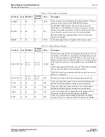
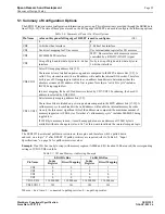
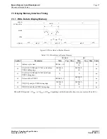
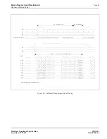
MEMW# Timing
Figure 12: MEMW# Timing (68000)
Where MCLK period = 1/f
OSC
, or 2/f
OSC
, or 4/f
OSC
depending on which mode the chip is in. (see section 9.2 and 9.3).
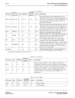
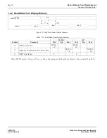
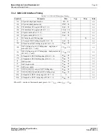
Table 7-3: MEMW# Timing (68000)
3V/3.3V
5V
Symbol
Parameter
Min
Typ
Max
Min
Typ
Max
Units
t1
AB[19:1] and MEMCS# valid before AS# falling edge
0
0
ns
t2
AB[19:1] and MEMCS# hold from AS# rising edge
0
0
ns
t3
AS# falling edge to DTACK# falling edge
3.5 *
MCLK
+ 20
3.5 *
MCLK
+ 10
ns
t4
AS# rising edge to DTACK hi-z delay
45
22
ns
t5
AS# falling edge to DB[15:0] valid
120
140
ns
t6
DB[15:0] hold from AS# rising edge
0
0
ns
AB[19:1]
AS#
UDS#/LDS#
VALID
VALID
t1
t3
t6
t2
t5
t4
DB[15:0]
MEMCS#
R/W#
DTACK#
Hi-Z
Hi-Z
Hi-Z
Hi-Z
INVALID