


Epson Research and Development
Page 23
Vancouver Design Center
Hardware Functional Specification
SED1352
Issue Date: 99/07/28
X16-SP-001-16
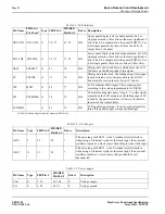
MEMR#
I
89
86
TTLS
Active low input to read data from the display memory. This pin
should be tied to V
DD
in an MC68000 MPU interface.
READY
O
90
87
TS3
For MC68000 MPU interface, this pin is connected to the
DTACK# pin of MC68000 and is driven low when ever a data
transfer is complete. In other bus interfaces, this output is driven
low to force the system to insert wait states when needed.
READY is placed in a high impedance (Hi-Z) state after the
transfer is completed.
RESET
I
32
29
TTLS
Active high input to force all signals to their inactive states.
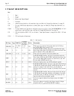
Table 5-2: Display Memory Interface
Pin Name
Type F0B Pin #
F1B/D0B
Pin/Pad #
Driver
Description
VD0-VD15 I/O
44 - 51,
54 - 61
41 - 48,
51 - 58
TS2D2
These pins are connected to the display memory data bus. For 16-
bit interface, VD0-VD7 are connected to the display memory data
bus of even byte addresses and VD8-VD15 are connected to the
display memory data bus of odd byte addresses. The output drivers
of these pins are placed in a high impedance state when RESET is
high.
On the falling edge of RESET the values of VD0-VD15 are latched
into the chip to configure various hardware options.
VD0-VD15 each have an internal pull-down resistor (see section
Table 5-6: on page 25).
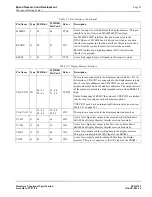
VA0-VA15 O
33 - 43,
62 - 66
30 - 40
59, 63
CO2
These pins are connected to the display memory address bus.
VCS1#
O
69
66
CO2
Active low chip-select output to the second or odd byte address
SRAM. See Display Memory Interface section for details.
VCS0#
O
68
65
CO2
Active low chip-select output to the first or even byte address
SRAM. See Display Memory Interface section for details.
VWE#
O
67
64
CO2
Active low output used for writing data to the display memory.
This pin is connected to the WE# input of the SRAMs.
VOE#
O
83
80
CO2
Active low output to enable reading of data from the display
memory. This pin is connected to the OE# input of the SRAMs.
Table 5-1: Bus Interface (Continued)
Pin Name
Type F0B Pin #
F1B/D0B
Pin/Pad #
Driver
Description