


Page 24
Epson Research and Development
Vancouver Design Center
SED1352
Hardware Functional Specification
X16-SP-001-16
Issue Date: 99/07/28
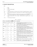
a
VESA Flat Panel Display Interface Standard (FPDI-1
TM
)
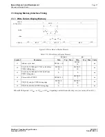
Table 5-3: LCD Interface
Pin Name
FPDI-1
TM
Pin Name
a
Type
F0B Pin #
F1B/D0B
Pin/Pad #
Driver Description
UD3-UD0
UD3-UD0
O
70 - 73
67 - 70
CO4
Upper panel display data for dual panel mode. For
single panel mode, these bits are the most significant 4
bits of the 8-bit output data to the panel (PD[4:7]). For
4-bit single panel mode, these bits are the 4 bits of
output data to the panel.
LD3-LD0
LD3-LD0
O
74 - 77
71 - 74
CO4
Lower panel display data for dual panel mode. For 8-bit
single panel mode, these bits are the least significant 4
bits of the 8-bit output data to the panel (PD[0:3]). For
4-bit single panels, these bits are driven 0 (low state).
XSCL
FPSHIFT
O
81
78
CO4
Display data shift clock. Data is shifted into the LCD
X-drivers on the falling edge of this signal.
LP
FPLINE
O
79
76
CO4
Display data latch clock. The falling edge of this signal
is used to latch a row of display data in the LCD X-
drivers and to turn on the row driver (Y driver).
WF
MOD
O
80
77
CO4
LCD backplane BIAS signal. This output toggles
according to the value programmed in AUX[05h].
YD
FPFRAME O
78
75
CO4
Vertical scanning start pulse. A logic ‘1’ on this signal,
sampled by the LCD module on the falling edge of LP,
is used by the panel row driver (Y driver) to indicate
the start of the vertical frame.
LCDENB
O
82
79
CO2
LCD enable signal output. It can be used externally to
turn off the panel supply voltage and backlight.
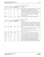
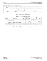
Table 5-4: Clock Inputs
Pin Name
Type
F0B Pin #
F1B/D0B
Pin/Pad #
Driver
Description
OSC1
I
92
89
*
This pin, along with OSC2, is the 2-terminal crystal interface
when using a 2-terminal crystal as the clock input. If an external
oscillator is used as a clock source, then this pin is the clock input.
OSC2
O
93
90
*
This pin, along with OSC1, is the 2-terminal crystal interface
when using a 2-terminal crystal as the clock input. If an external
oscillator is used as a clock source this pin should be left
unconnected.
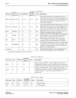
Table 5-5: Power Supply
Pin Name
Type
F0B Pin #
F1B/D0B
Pin/Pad #
Driver
Description
V
DD
P
3, 53
50, 100
P
Voltage supply.
V
SS
P
2, 52
49, 99
P
Voltage ground.