


Epson Research and Development
Page 13
Vancouver Design Center
Programming Notes and Examples
SED1352
Issue Date: 98/10/08
X16-BG-007-04
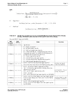
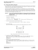
AUX[0Eh]
0000 0100
increment palette address
AUX[0Fh]
0000 0000
write monochrome LUT data
AUX[0Eh]
0000 0101
increment palette address
AUX[0Fh]
0000 0101
write monochrome LUT data
AUX[0Eh]
0000 0110
increment palette address
AUX[0Fh]
0000 1010
write monochrome LUT data
AUX[0Eh]
0000 0111
increment palette address
AUX[0Fh]
0000 1111
write monochrome LUT data
AUX[0Eh]
0000 1000
increment palette address
AUX[0Fh]
0000 0000
write monochrome LUT data
AUX[0Eh]
0000 1001
increment palette address
AUX[0Fh]
0000 0101
write monochrome LUT data
AUX[0Eh]
0000 1010
increment palette address
AUX[0Fh]
0000 1010
write monochrome LUT data
AUX[0Eh]
0000 1011
increment palette address
AUX[0Eh]
0000 1111
increment palette address
AUX[0Fh]
0000 1100
write monochrome LUT data
AUX[0Fh]
0000 0000
write monochrome LUT data
AUX[0Eh]
0000 1101
increment palette address
AUX[0Fh]
0000 0101
write monochrome LUT data
AUX[0Eh]
0000 1110
increment palette address
AUX[0Fh]
0000 1010
write monochrome LUT data
AUX[0Eh]
0000 1111
select palette address
AUX[0Fh]
0000 1111
write monochrome LUT data
AUX[01h]
1001 1000
Program Mode Register bit DISP to 1, and set LCDE to enable
power supply.
1001 0000b ‘OR’ {original value for AUX[01h]}
•
b7 = display on (application specific)
•
b4 = LCDE = LCDENB pin = set to enable specific power supply
design (for SDU1353B0C, set bit to 1 to enable power supply)
(application specific)
Write one pixel to the top left corner of display memory.
If the SDU1352B0x evaluation board is used, the first panel’s memory addresses begin at C000:0000h (see Section 5.4.4.1,
“Displaying a Single Image on a Dual Panel” on page 40). Consequently write 0C0h to location C000:0000h for the
SDU1352B0x.
AUX
Register
Data
(in Binary)
Notes
See Also