


Epson Research and Development
Page 13
Vancouver Design Center
SDU1352B0C Rev. 1.0 Evaluation Board User Manual
SED1352
Issue Date: 98/10/07
X16-AN-002-09
1.3.2 Non-ISA Bus Support
This evaluation board was specifically designed to support the standard 8-/16-bit ISA bus. However, as the SED1352 does
support other bus interfaces, header strips have been provided containing all necessary I/O pins (see section 1.3.9 on page
14).
When using the header strips to provide the bus interface observe the following:
1.
All I/O signals on the ISA bus card edge must be isolated from the ISA Bus (do not plug the card into a computer).
Voltage lines are provided on the header strips.
2.
U2, a TIBPAL22V10, is currently used to provide the SED1352 IOCS# (pin 23) and MEMCS# (pin 22) input signals
for ISA bus use. This functionality must now be provided externally and these two pins need to disconnected as there
may be conflict problems associated with two different outputs driving the same input.
1.3.3 SRAM Support
The SDU1352B0C board supports 16-bit wide, 64K byte - 128K byte SRAM only. DIP switch SW1-8 selects between the
two options.
1.3.4 Monochrome LCD Support
The SED1352 supports 4- and 8-bit Dual and Single monochrome STN LCD panels. All the necessary signals are provided
on the 40-pin ribbon cable header. The interface signals are alternated with grounds on the cable to reduce cross talk and
noise related problems.
Refer to Table 1-4, “LCD Signal Connector J1 Pinout,” on page 9 for specific settings.
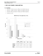
1.3.5 Power Save Modes
The SED1352 supports 2 software Power Save Modes. The utility program 1352PD.EXE is supplied to control the software
modes. The software modes are controlled by directly writing the SED1352 associated internal registers.
1.3.6 Adjustable LCD Panel Negative Power Supply
The majority of Monochrome LCD panels require a negative power supply to provide between -18 V and -23 V
(I
out
=45mA). For ease of implementation, such a power supply has been provided as an integral part of this design. The
signal VLCD can be adjusted by R11 (100K potentiometer) to provide an output voltage from -14 V to -23 V and is
enabled/disabled by the control signal LCDENB.
Note
LCDENB is directly controlled by register AUX[01], bit 4, of the SED1352. The VLCD power supply used on the
SDU1352 requires a logic “1” to disable it. As the signal LCDENB is a logic “0” at power-up, it is inverted by ex-
ternal logic to disable VLCD and prevent damaging the panel connected to the SDU1352.
Determine the panel’s specific power requirements and set the potentiometer accordingly before connecting the panel.