


Page 16
Epson Research and Development
Vancouver Design Center
SED1352
Hardware Functional Specification
X16-SP-001-16
Issue Date: 99/07/28
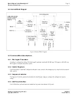
3.3.5 Look-Up Table
The Look-Up Table contains sixteen 4-bit wide palettes that can be configured as one 16x4 palette, or four 4x4 palettes
used for the re-mapping of gray-scale outputs. See “Look-Up Table Architecture” on page 54.
3.3.6 Port Decoder
According to configuration settings VD1, VD12 - VD4, IOCS# and address lines AB9-1, the Port Decoder validates a given
I/O cycle.
3.3.7 Memory Decoder
According to configuration settings VD15 - VD13, MEMCS# and address lines AB19-17, the Memory Decoder validates
a given memory cycle.
3.3.8 Data Bus Conversion
According to configuration setting VD0, the Data Bus Conversion maps the external data bus, either 8-bit or 16-bit, into
the internal odd and even data bus.
3.3.9 Address Generator
The Address Generator generates display refresh addresses used to access display memory.
3.3.10 CPU / CRT Selector
The CPU / CRT Selector accesses the display memory from the CPU or the display refresh circuitry.
3.3.11 Display Data Formatter
The Display Data Formatter reads the display data from the display memory and outputs the correct format for all supported
LCD panel types and gray scale selections.
3.3.12 Clock Inputs / Timing
Clock Inputs / Timing generates the internal master clock according to the gray-level selected and display memory
interface. The master clock (MCLK) can be:
- MCLK = input clock
- MCLK = 1/2 input clock
- MCLK = 1/4 input clock
Refer to section 9.2 SRAM Access Time for further details
Pixel clock = input clock.
3.3.13 SRAM Interface
The SRAM Interface generates the necessary signals to interface to the Display memory (SRAM).