5: Mixer Board
PRC1099A-MS
5-3
Down-
Conversion Mixer
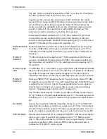
Double-balanced mixer MX1 mixes the 75 MHz IF signal with the 76.6 to
105 MHz first local oscillator (LO1) from the LO1 input (SYN1) from the
Synthesizer board to produce an audio-modulated transmit signal at the
selected channel frequency. MX1 runs at a very low-level to minimize
spurious outputs.
30 MHz
Low-Pass Filter
At the output of RF mixer MX1, the 30 MHz low-pass filter, consisting of C9,
L3, C10, L4, and C11 removes the image frequency as well as unwanted
image and spurious responses above 30 MHz. These spurious responses are
produced from mixing the 75 MHz IF signal with LO1.
Amplifier 1.6 to
30 MHz
The low-level transmit output from double-balanced mixer MX1 is amplified
by MMIC (monolithic, microwave, integrated circuit) U1, providing a stable
50 ohms to 50 ohms amplification over a very wide frequency range without
any external components.
Current
Regulator
MMIC (U1) is designed to operate from a 20V supply using a series bias
resistor in the supply load. Since the PRC1099A is designed to operate over a
supply range in excess of 10V to 15V, current regulator U3 provides a
constant current source for U1. The current output is determined by R60 and
R61. The current to U1 is switched on by TX gate Q5 that is controlled by the
R8 line.
Transmit/Receive
Switch
The transmit signal is output to the PA board through the transmit/receive
(T/R) switch controlled by relay K1. The relay is activated by T8 (+8V). The
transmit signal is output at the TX OUT terminal.
5.1.2
Receive Mode
In receive mode, the Mixer board receives the receive signal from the
Audio/Filter board on the RX IN terminal and applies it to the 30 MHz
low-pass filter circuit after being switched through T/R switch by relay K1.
30 MHz Low-
Pass Filter
The low-pass filter consisting of C9, L3, C10, L4, and C11, located at the
input of RF mixer MX1, removes the unwanted image and spurious responses
above 30 MHz from the receive signal before being mixed with the local
oscillator frequency.
Squelch Gates
For battery powered manpack configurations, power conservation is a
constant design consideration. Squelch gates Q2 and Q4 provide a way to
reduce the LO1/mixer circuit current drain in receive mode when squelch is
turned on (receive signal is muted).
Note:
When referring to squelch states in this manual, “squelch is turned
on
,”
means the same as “squelch is
closed
. Conversely, “squelch is turned
off
,” means the same as “squelch is
open
.” When squelch is turned
on
, the receive signal is muted. When squelch is turned off, the
receive signal is unmuted. When the receive signal includes voice
modulation, squelch is broken and temporarily switches from
on
or
closed
to
off
or
open
.
Содержание PRC1099A
Страница 4: ......
Страница 8: ......
Страница 35: ......
Страница 49: ...3 Audio Filter Board 3 14 PRC1099A MS Figure 3 2 Audio Filter Board Component Locations 738221 Rev J ...
Страница 65: ......
Страница 71: ...4 1650 kHz IF Board 4 6 PRC1099A MS Figure 4 2 1650 kHz IF Board Component Locations 738028 Rev D ...
Страница 76: ......
Страница 86: ...5 Mixer Board 5 10 PRC1099A MS Figure 5 4 Mixer Board Component Locations 738217 Rev H ...
Страница 97: ......
Страница 103: ...6 Power Amplifier Board 6 6 PRC1099A MS Figure 6 2 Power Amplifier Board Component Locations 738617 Rev C ...
Страница 117: ...7 Antenna Tuner Board PRC1099A MS 7 9 Figure 7 2 Antenna Tuner Driver Board Component Locations 738346 Rev B ...
Страница 118: ...7 Antenna Tuner Board 7 10 PRC1099A MS Figure 7 3 Antenna Tuner Board Component Locations 738027 Rev D ...
Страница 125: ......
Страница 131: ...8 Synthesizer Board 8 6 PRC1099A MS Figure 8 2 Synthesizer Board Component Locations 738025 Rev A ...
Страница 163: ...9 Processor Board 9 14 PRC1099A MS Figure 9 2 Processor Board Component Locations 738218 Rev B ...
Страница 178: ...10 Display Board 10 8 PRC1099A MS Figure 10 1 Display Board Component Location Diagram 738220 Rev G ...
Страница 181: ......
Страница 185: ...11 Junction Board 11 4 PRC1099A MS Figure 11 1 Junction Board Component Locations 738222 Rev F ...
Страница 200: ......
Страница 207: ...13 Internal Options PRC1099A MS 13 7 Figure 13 3 ALE Board Component Locations 1 of 2 738215 Rev B ...
Страница 208: ...13 Internal Options 13 8 PRC1099A MS Figure 13 4 ALE Board Component Locations 2 of 2 738215 Rev B ...
Страница 241: ......
Страница 247: ...Index 6 T Technical specifications 1 2 Transmit path 2 4 U USB 1 4 see also Modulation modes USB LSB mode V VSWR 1 4 ...


