5: Mixer Board
5-2
PRC1099A-MS
5.1.1
Transmit Mode
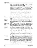
The single sideband transmit signal is received from the 1650 kHz IF board at
the 1650 kHz terminal. From the 1650 kHz terminal, the SSB transmit signal
is applied to mixer U2.
Up-Conversion
Mixer
This stage up-converts the 1650 kHz SSB signal to 75 MHz. Active
double-balanced mixer U2 mixes the 1650 kHz IF (USB mode) signal with
the 73.35 MHz second LO from the Synthesizer board to produce the 75 MHz
IF signal. Potentiometer R37 sets the mixer gain. In transmit mode, PIN diode
D13 is forward-biased by T8 (+8V), enabling the 1650 kHz IF input signal to
be applied to mixer U2. The 75 MHz IF output is coupled to Q11 through the
filter formed by C64, L22, and variable capacitor C65.
LO2 Buffer
Second local oscillator buffer Q10 amplifies the low level 73.35 MHz LO2
input from the Synthesizer board to an output level of 2 Vrms. Tuned output
circuit L20 and variable capacitor C58 insure good spectral purity. In transmit
mode, the level is dropped to 100 mV through R43 for injection into transmit
mixer U2.
TX Gain
Controlled
Amplifier
Dual gate MOSFET amplifier Q11 integrates the automatic level control
(ALC) signal from the Audio/Filter board to control the stage gain. The ALC
signal from Q12 is input at Q11 gate 2 (pin 3) with the 75 MHz IF signal at
gate 1 (pin 4).
The ALC signal received from Audio/Filter board is applied to ALC amplifier
Q12 (refer to “ALC Circuit” on page 3-6). When the ALC circuit is not active,
a maximum voltage of 4V is applied to gate 2 through voltage divider R54 and
R55.
The drain of Q11 is connected through broadband transformer T4 to the
50 ohm input of the 75 MHz filter through PIN diode switch D11. D11 is
forward-biased in transmit mode by T8 (+8V) through R33, R34, and T4.
75 MHz Filter
In transmit mode, 75 MHz filter Y1 rejects the image output from mixer U2
and provides additional attenuation of the LO2. The output from the 75 MHz
filter passes through a tuned matching network consisting of C18, L5, and
C17 that matches the high impedance crystal filter with the resonant tank
circuit of L6 and C24. PIN diodes D1 and D2 act as T/R switches directing the
transmit signal from the LC matching network to the resonant tank circuit of
C24, L6, and then to double-balanced mixer MX1. T8 forward-biases D1 and
D2 in transmit mode; R8 reverse-biases D1 and D2 in receive mode.The
transmit signal bypasses the RX IF amplifier U4.
LO1 Buffer
First local oscillator buffer Q1 amplifies the low-level DDS synthesizer LO1
output to a level of approxi7 dBm for injection into the 50 ohm
oscillator port of MX1. The output from Q1 is coupled to mixer MX1 through
broadband transformer T1 and 105 MHz, low-pass, LC filter C6, L2, and
C7. The response is substantially flat over the Q1 output range of 76.6 to
105 MHz.
π
π
Содержание PRC1099A
Страница 4: ......
Страница 8: ......
Страница 35: ......
Страница 49: ...3 Audio Filter Board 3 14 PRC1099A MS Figure 3 2 Audio Filter Board Component Locations 738221 Rev J ...
Страница 65: ......
Страница 71: ...4 1650 kHz IF Board 4 6 PRC1099A MS Figure 4 2 1650 kHz IF Board Component Locations 738028 Rev D ...
Страница 76: ......
Страница 86: ...5 Mixer Board 5 10 PRC1099A MS Figure 5 4 Mixer Board Component Locations 738217 Rev H ...
Страница 97: ......
Страница 103: ...6 Power Amplifier Board 6 6 PRC1099A MS Figure 6 2 Power Amplifier Board Component Locations 738617 Rev C ...
Страница 117: ...7 Antenna Tuner Board PRC1099A MS 7 9 Figure 7 2 Antenna Tuner Driver Board Component Locations 738346 Rev B ...
Страница 118: ...7 Antenna Tuner Board 7 10 PRC1099A MS Figure 7 3 Antenna Tuner Board Component Locations 738027 Rev D ...
Страница 125: ......
Страница 131: ...8 Synthesizer Board 8 6 PRC1099A MS Figure 8 2 Synthesizer Board Component Locations 738025 Rev A ...
Страница 163: ...9 Processor Board 9 14 PRC1099A MS Figure 9 2 Processor Board Component Locations 738218 Rev B ...
Страница 178: ...10 Display Board 10 8 PRC1099A MS Figure 10 1 Display Board Component Location Diagram 738220 Rev G ...
Страница 181: ......
Страница 185: ...11 Junction Board 11 4 PRC1099A MS Figure 11 1 Junction Board Component Locations 738222 Rev F ...
Страница 200: ......
Страница 207: ...13 Internal Options PRC1099A MS 13 7 Figure 13 3 ALE Board Component Locations 1 of 2 738215 Rev B ...
Страница 208: ...13 Internal Options 13 8 PRC1099A MS Figure 13 4 ALE Board Component Locations 2 of 2 738215 Rev B ...
Страница 241: ......
Страница 247: ...Index 6 T Technical specifications 1 2 Transmit path 2 4 U USB 1 4 see also Modulation modes USB LSB mode V VSWR 1 4 ...


